Depending on the environment in which a device is used, the DC voltage powering it may fluctuate, producing AC voltage ripples and noise. This can significantly degrade its performance if proper power filtering and bypassing is not used. Any IC has the ability to reject the supply ripples and noise to a certain degree, which is represented with its Power Supply Rejection Ratio (PSRR). The PSRR is the measure of the device’s sensitivity with respect to power supply variations and will eventually dictate the IC’s performance. No matter how good the IC’s PSRR is, the power supply voltage must be kept as clean as possible from AC voltage ripples and noise to preserve its performance. This can be achieved by using appropriate decoupling capacitors and, eventually, ferrite beads.
The role of the decoupling capacitors is to dampen the AC voltage ripple and noise on the power supply line by charging and discharging to compensate for them, which can be seen as providing a low impedance path to ground to those undesirable fluctuations. As the frequency of the fluctuations and noise can vary from low to high, a set of capacitors—three in general—is necessary to achieve that goal. A first large capacitor acts as a filter that takes care of the low frequency noise and ripples, and prevents voltage droops due to high current switching. A second smaller capacitor should reduce the higher frequency noise, and a third even smaller capacitor should reduce the highest frequency noise and prevent instability that can be created by the device rapidly switching as it provides energy to fast switching transitions.
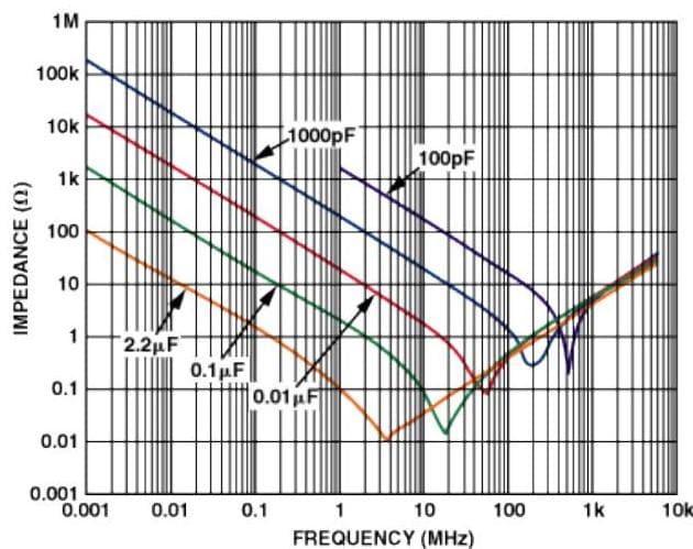
Figure 1 shows frequency response plots for same-size capacitors with different capacitance values. At low frequency, the capacitive reactance is dominant, while at high frequency, the inductive reaction is dominant. The dip is where they compensate each other and the impedance is just the ESR of the capacitor. The lower the capacitance, the higher frequency is in the dip position. Based on such characteristics and knowing the frequency band of the ripples and noise that need to be reduced or removed from the power supply line, one can choose the approximate decoupling capacitor values.
Figure 1. Example of Capacitor Frequency Response.
Figure 2 shows a commonly used filter circuit in which the 10 uF (could range from 4.7 uF to 47 uF) capacitor acts as a charge reservoir that prevents large voltage droops and minimizes low frequency noise on the power supply line, while the 1 uF decoupling capacitor reduces high frequency noise. The 0.01 uF bypass capacitor reduces even higher frequency noise and must be placed as close as possible to the power pin of the device to provide a fast response to the transient currents when the device is switching in order to prevent instabilities. If the power source is too noisy and/or the device is producing too much switching noise, a ferrite bead can be used to add more isolation to protect the power plane from the switching noise of the device and also protect the device from the excessive noise coming from the power plane. Figure 3 shows the circuit of Figure 2 with added ferrite bead.

Figure 2. Supply Filter and Bypass.

Figure 3. Supply Filter and Bypass with Ferrite Bead.
If the device has multiple power pins and is used in a high-density board with many other devices, each category of power pins, for example VDD, VDDO, VDDA should have their own local power plane for better isolation. Each local power plane connects to the main plane through a filter comprised from decoupling capacitors and ferrite bead and each power pin will have its own bypass capacitor as shown in Figure 4.

Figure 4. Power Filtering for a Device with Multiple Power Pins.
For greater efficiency, select capacitors with low equivalent series resistor (ESR) and low equivalent series inductance (ESL) such as electrolytic and ceramic capacitors. The ferrite bead selection should be based on the following factors:
Impedance vs frequency characteristics. The best results are obtained if the target noise frequency falls within the bead resistive band (resistive impedance dominates the reactive impedance) and that resistive impedance is chosen to be as high as possible for greater noise attenuation.
As the impedance vs frequency characteristic shifts with current (Figure 5), the operating current should be known in order to select the ferrite bead with the desired impedance. Also, the maximum current from the spec should be at least twice the current of operation in the application to preserve the ferrite bead efficiency.
The DC impedance should be the lowest possible as it causes a drop in the supply voltage which could become significant with low supply voltage such as 1.2 V.

Figure 5. Example of Ferrite Bead Impedance Change with Current.
The capacitors should be placed as close as possible to the power pin of the chip, one inch or closer. The main function of the small cap (0.01 uF in the example) is to store charge to provide energy to the higher frequency switching transitions. Therefore, it must be placed as close as possible to the power pin for minimum inductance and more efficiency.
The capacitors should be directly connected to the power planes through vias and very short traces to minimize the inductance in that path to low inductance power planes.
Just connect the power pin to the main power plane and install the caps as shown in Figure 6.

Figure 6. Decoupling Capacitor Placement and Routing for Chip with a Single Power Pin.
If the chip has different functional blocks that require isolation from each other—like an analog block, digital block, and output block—it’s recommended to create a local power plane for each of them. The local power plane is just an isolated cut out from the main power plane and connects to it through vias and decoupling capacitors (and eventually ferrite bead) as shown on the example of Figure 7.
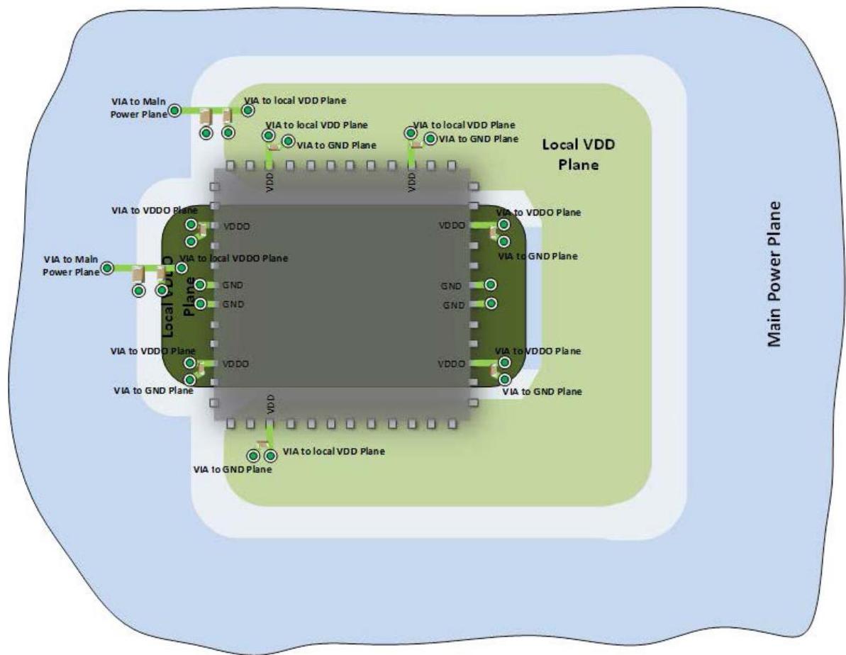
Figure 7. Decoupling Capacitor Placement and Routing for Chip with Multiple Power Pins.