Today’s fanless programmable logic controller (PLC) and IO-Link® gateway systems must dissipate large amounts of power depending on the I/O configuration (IO-Link, digital input/output, analog input/outputs). As these PLCs evolve into new Industry 4.0 smart factories, special attention must be considered to achieve smarter, faster, and lower power solutions. At the heart of this revolution is an exciting new technology called IO-Link, which enables flexible manufacturing to improve factory throughput and operational efficiency. This exciting new technology enables traditional sensors to become intelligent sensors.
At Analog Device, we provide a portfolio of advanced factory automation solutions that create pathways toward achieving Industry 4.0, enhanced by our IO-Link technology portfolio. A recent addition to this portfolio is the MAX22513, a tiny dual-channel IO-Link transceiver with integrated surge protection and a DC-to-DC converter, to reduce heat dissipation and increase the robustness of sensors on the factory floor.
To help our customers reduce their time to market, we have partnered with software stack vendors from the IO-Link consortium to develop a range of fully verified and tested reference designs, which are described in detail in this handbook.
IO-Link is a powerful technology that will play a pivotal role over time in factory process automation as well as other industries. It will not only save manufacturers billions every year but will expand new markets for more customization of products. If you are involved in factory process automation, watch IO-Link technology as it continues to unleash the true power of Industry 4.0 and changes the way we think of manufacturing.
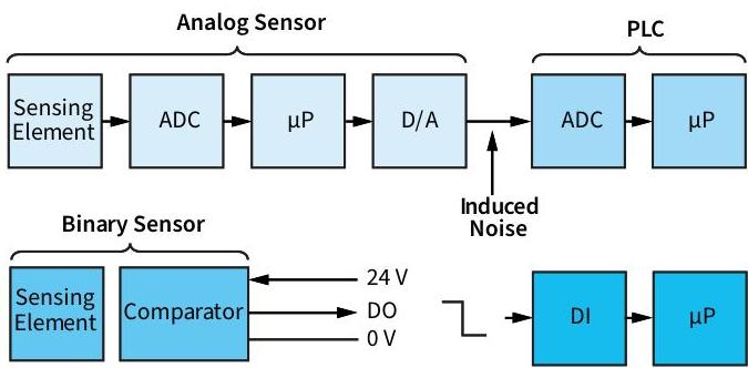
Historically, a sensor included a sensing element and a way to get the sensing data to a controller. Data was often transferred in analog format (Figure 1) and was unidirectional (sensor to controller only). This added extra steps to the process (such as digital-to-analog and analog-to-digital conversion) that, in turn, added extra cost, larger footprints, and susceptibility to noise. Binary (or digital) sensors were used to simply indicate the status of a switch; for example, a thermostat to provide a high (24 V) or low (0 V) signal to indicate if the measured temperature is above or below a preset threshold. These „old school“ sensors worked, but as technology advanced, sensor manufacturers integrated more functionality into sensors, eliminating some of these problems with these early sensors.
However, data was still limited to unidirectional communication from the sensor to the master, limiting error control and requiring a technician on the factory floor for updates or recalibration.
Manufacturers needed a better solution to meet the demands of Industry 4.0, smart sensors, and reconfigurable factory floors. The solution that emerged is IO-Link.
Figure 1. „Old School“ sensors: analog and binary.
Binary sensors have only two states: on or off. Examples of binary sensors are pressure switches, temperature switches, through-beam photoelectric sensors, proximity sensors, and pushbuttons. Binary sensor output drivers, such as the MAX14838/MAX14839 (Figure 2), are 24 V/100 mA drivers optimized for use in industrial sensors. These devices integrate the high voltage (24 V) circuitry commonly found in industrial sensors, such as a configurable or pin-selectable PNP/NPN/push-pull driver and an integrated linear regulator that meets common sensor power requirements. The output driver interfaces between the sensor or sensor microcontroller unit (MCU) and the digital input (DI) module of the PLC.
To provide flexibility in supporting a broad range of physical sensor types, logic inputs allow the output driver to be configured for high-side (PNP), low-side (NPN), or push-pull operation. An additional input allows the user to select between normally open and normally closed logic. The MAX14838/MAX14839 are highly integrated products, making them ideal for robust sensor solutions in a tiny footprint due to integrated reverse-polarity protection, an on-board LDO regulator, and LED drivers.

Figure 2. A 24 V pin-configurable industrial sensor output driver.
IO-Link is a standardized technology (IEC 61131-9) regulating how sensors and actuators in industrial systems interact with a controller. The IO-Link Company Community (io-link.com) was formed in 2008 by a group of 41 sensor and actuator manufacturers who started the IO-Link consortium with the goal to standardize the hardware (PHY layer) interface and the communication (data) protocol for IO-Link products. Currently, there are over 100 companies in the consortium including semiconductor vendors and software vendors. Maxim, now part of ADI, has been a member of the IO-Link consortium since 2009.
IO-Link is a point-to-point communication link with standardized connectors, cables, and protocols. The IO-Link system is designed to work within the industry-standard 3-wire sensor and actuator infrastructure and is comprised of IO-Link master and IO-Link device products (Figure 3).

Figure 3. IO-Link master/device interface.
The number of installed IO-Link nodes continues to rapidly grow as sensor companies move from older analog sensors to smart IO-Link-based sensors, enabling the promise of reconfigurable manufacturing as outlined by Industry 4.0 (Figure 4).

Figure 4. Growth in the number of IO-Link nodes installed.
The point-to-point connection between the IO-Link master (multiport controller or gateway) and the IO-Link device (sensor or actuator) uses standard connectors (usually M12) and a 3- or 4-wire cable up to 20 meters in length. The master can have multiple ports (commonly four or eight). Each port of the master connects to a unique IO-Link device, which can operate in either SIO mode or bidirectional communication mode. IO-Link is designed to work with existing industrial architectures such as fieldbus or Industrial Ethernet and connects to existing PLCs or human-machine interfaces (HMIs), enabling rapid adoption of this technology (Figure 5).
For full details of IO-Link, refer to the IO-Link Interface and System Specification Version 1.1.3 dated June 2019 at io-link.com.

Figure 5. IO-Link compatibility with existing industry protocols.

Figure 6. IO-Link pin definitions.
IO-Link is a standard for single-drop communication interface (SDCI), which was standardized as IEC 61131-9, while also providing backward-compatibility with binary sensors IEC 60974-5-2 (Figure 6 and Table 1). IO-Link sensors have the best features of binary sensors while adding bidirectional data capability. IO-Link masters can interface with both binary and IO-Link sensors, allowing IO-Link to be easily added to an existing system. The IO-Link standard states that communications must be within 20 meters with unshielded cables using standard connectors common to industrial systems. M8 and M12 connectors are the most predominant. Communication is point-to-point and requires a 3-wire interface (L+, C/Q, and L-). Communication between an IO-Link master and device is half-duplex with three transmission rates: COM1 4800 baud, COM2 38.4 kbaud, and COM3 230.4 kbaud.
The supply range in an IO-Link system is 20 V to 30 V for the master, and 18 V to 30 V for the device (sensor or actuator). The IO-Link device must function within 300 ms after L+ exceeds the 18 V threshold.
The two communication modes are standard I/O (SIO) and SDCI. SIO mode ensures backward
compatibility with existing sensors in the field, using 0 V or 24 V to signal OFF or ON to the IO-Link master. In IO-Link mode, communication is bidirectional at one of three data rates. The IO-Link device only supports one data rate while the IO-Link master must support all three data rates. Communication is with 24 V pulses using a nonreturn-to-zero (NRZ) coding scheme on the C/Q line where a logic 0 is 24 V between CQ and L- and a logic 1 is 0 V between CQ and L-. In IO-Link mode, pin 2 can be in DI mode as a digital input, or DO mode as a digital output, or not connected (NC).
Table 1. IO-Link Pin Definitions
| Pin | Signal | Designation | Standard |
|---|---|---|---|
| 1 | L+ | 24 V | IEC 61131-2 |
| 2 | I/Q | Not connected, DI, or DO | IEC 61131-2 |
| 3 | L- | 0 V | IEC 61131-2 |
| 4 | Q | Switching signal (SIO) | IEC 61131-2 |
| C | Coded switching (COM1, COM2, COM3) | IEC 61131-9 |
Standardized connectors and cables are used as defined by IEC 61131-9. Port Class A connectors have 4-wire connections (maximum) to support the 3-wire connection system (L+, L-, C/Q) with a fourth wire that can be used as an additional signal line (DI or DO). Port Class B connectors have 5-wire connections for devices that require extra power from an independent 24 V supply (Figure 7 and Table 2).
Table 2. Alternative IO-Link Pin Definitions
| Pin | Signal | Designation | Remark |
|---|---|---|---|
| 1 | L+ | Power supply (+) | See Table 7* |
| 2 | I/Q | ||
| P24 | NC/DI/DO (port class A) | ||
| P24 (port class B) | Option 1: NC (not connected) | ||
| Option 2: DI; Option 3: DI, then configured DO | |||
| Option 4: Extra power supply for power devices (port class B) | |||
| 3 | L- | Power supply (-) | See Table 7* |
| 4 | C/Q | SIO/SDCI | Standard I/O mode or SDCI |
| 5 | NC N24 | NC (port class A) | |
| N24 (port class B) | Option 1: Shall not be connected on the master side (port class A) | ||
| Option 2: Reference to the extra power supply (port class B) |

Figure 7. Alternative IO-Link connectors.
The supply range in an IO-Link system is 20 V to 30 V for the master, or 18 V to 30 V for the device (sensor or actuator). Important related specifications (Table 3) include:
Note that the high and low detection time (t_H and t_L in the timing diagram) are 1/16 of a bit (minimum). t_NO is the noise suppression duration (t_NO must be less than 1/16 of a bit) (Figures 8a and 8b).
Communication uses a UART frame consisting of 11 bits = 1 start bit + 8 data bits + 1 parity bit + 1 STOP bit. Durations are defined by the transmission rate, which depends upon the device.
Table 3. IO-Link Signal Electrical Specifications
| Property | Designation | Min | Typ | Max | Unit | Remark |
|---|---|---|---|---|---|---|
| VTHH_{D,M} | Input threshold ‚H‘ | 10.5 | N/A | 13 | V | See Note 1 |
| VTHL_{D,M} | Input threshold ‚L‘ | 8 | N/A | 11.5 | V | See Note 1 |
| VHYS_{D,M} | Hysteresis between input thresholds ‚H‘ and ‚L‘ | 0 | N/A | N/A | V | Shall not be negative. See Note 2 |
| VIL_{D,M} | Permissible voltage range ‚L‘ | VO_{D,M} – 1.0 | N/A | N/A | V | With reference to relevant negative supply voltage. |
| VIH_{D,M} | Permissible voltage range ‚H‘ | N/A | N/A | V+_{D,M} +1.0 | V | With reference to relevant positive supply voltage. |
Note 1: Thresholds are compatible with the definitions of type 1 digital inputs in IEC 61131-2.
Note 2: Hysteresis voltage $V_{HYS} = V_{THH} – V_{THL}$.

(a)

(b)
Figure 8. (a) IO-Link signal electrical thresholds; (b) IO-Link signal electrical characteristics.
An IO-Link device is connected as a point-to-point link to a port in an IO-Link master. If implemented as a PLC plug-in module, it does not have gateway functionality and as such, is not a fieldbus. The IO-Link master is essentially a gateway, with responsibility for establishing communication using fieldbuses or some other type of backplane, enabling the IO-Link devices to become fieldbus I/O nodes (Figure 9).
IO-Link functionality in a system reduces maintenance, increases uptime, and transforms a manual sensor installation into one that allows a user to „plug-and-play and walk away.“ The parameter settings can be
downloaded from the controller to set up (or reconfigure) a device. This means a technician is no longer needed on the shop floor to do initial setup and machine downtime is reduced when it is required to reconfigure devices.
IO-Link allows for continuous diagnostics and improved data logging and error detection to further reduce operating costs. Commonly used connectors and cables enable standardized installation with direct binary sensor upgrades. Since IO-Link sensors have configurable settings (for example, PNP, NPN, or push-pull outputs that can be changed while in progress), the number of product units the sensor vendor needs to support is also reduced.

Figure 9. IO-Link fieldbus interconnection.
To summarize, IO-Link is a point-to-point connection that may be layered over any given network. As an integral part of the I/O module, the IO-Link master is installed either in the control cabinet or directly in the field as a remote I/O with an IP 65/67 enclosure rating. The IO-Link device is coupled with the master using a standard sensor/actuator cable measuring up to 20 meters in length. The device—which may be any sensor, any actuator, or a combination of the two—transmits and receives data (binary switching, analog, input, output) that are transmitted directly via IO-Link in a digital format.
IO-Link is very powerful and flexible, allowing some of the intelligence to be moved from the PLC closer to the sensors on the factory floor. For example, by using Pin 2 (I/Q) as a DI/DO, in addition to the C/Q line, the user can take in digital input signals from a binary sensor and then drive a lamp with the DO (to signify, for instance, if a threshold has been surpassed). This can be done from the sensor itself.
As mentioned, IO-Link is backward-compatible with SIO binary signals. With IO-Link-capable sensors, users communicate with existing PLCs through a standard digital input communication. As PLC modules are upgraded with an IO-Link master, bidirectional communication is enabled through the C/Q line on an IO-Link channel. As PLC modules are upgraded with an IO-Link master, bidirectional communication is enabled through the C/Q line on an IO-Link channel.

Figure 10. Industrial sensor ecosystem.
Figure 10 shows an example of our industrial sensor ecosystem, which includes products for all key functions, including binary sensor output drivers, IO-Link devices, and IO-Link masters.
All IO-Link data exchange is master-device based, with the IO-Link master sending a request and the device required to answer. The data link layer manages the exchange of messages between the IO-Link master and device. Messages are called M-sequences, which are frames that have a length between 1 and 66 UART words. The messages can contain process data, on-request data, and system management commands/request. A special DL handler in the master manages operating modes (SIO, wake-up, COM rates) and handles errors and wake-up requests.
The process data handler ensures the cyclical process data exchange while the on-request
handler manages the acyclic exchange of event, control, parameter, and ISDU data.
IO-Link data communication is either cyclic or acyclic (Figure 11). Cyclic communication occurs during normal operation. For example, the master requests sensing data from the sensor. Acyclic data is on-request and can contain:
Event triggered, which is reported with three levels of severity:
Notifications
Errors
Service data for large data structures.

Figure 11. IO-Link transmission types.
All communication between the master and a device (sensor or actuator) begins with a request from the master and follows a fixed schedule (Figure 12). A device must answer all master requests. The sum of this back-and-forth communication is called an M-sequence (message sequence). An M-sequence can take many different forms and varies in total length. Although M-sequence communication may vary, all communication between a master and device takes place on this fixed schedule.
All data is UART framed. The master initiates communication and the device must answer within 1 TBit ≤ tA ≤ 10 TBit intervals (Figure 13).
When a master wants to configure a device (sensor or actuator) or communicate with it for
the first time, it will send a wake-up request. A wake-up request starts by shorting the C/Q line for 80 μs with a current pulse of at least 500 mA (Figure 14). The device must be ready for communication within 500 μs (TREN).

Figure 12. IO-Link master-device communication sequence.

Figure 13. UART framing.


Figure 14. Wake-up sequence.
Once the master has sent a wake-up request to the device (to set it to receive mode), the master then learns more about it by establishing the data rate for communication (Figure 15):
The device will respond at its rated data rate:
When the device responds, the master is then able to communicate with the device.
The master can then read out the minimum cycle time capability of the IO-Link device.
The master can retry the wake-up sequence a maximum of two times to establish IO-Link communication.

Figure 15. Data rate selection.
All IO-Link devices (sensors or actuators) must have an associated IO-Link Device Description (IODD) file available (Figure 16). This is used by the IO-Link master for purposes of identification, data interpretation, and configuration.
Device parameters
Identification information

Figure 16. IODD file.
In this section, we will look at reference design examples that demonstrate how to design a smart sensor system as well as a system to support legacy binary sensors that interface to an IO-Link port.
The basic structure of an IO-Link sensor includes some fundamental building blocks (Figure 17a and Figure 17b) that the system
designer must consider:

(a)

(b)
Figure 17. (a) Building blocks of an IO-Link sensor and (b) Building blocks of a highly integrated IO-Link sensor.
Figure 18 shows the MAXREFDES164 temperature sensor and the MAXREFDES171 distance sensor. The MAXREFDES173 temperature sensor and the MAXREFDES174 distance sensor are also discussed in this section. These designs are compliant with IO-Link version 1.1 and 1.0 and include transient voltage suppression as well as reverse-polarity and short-circuit protection. For MAXREFDES164, the IO-Link transceiver is the single-channel MAX14828, which is very low power but requires external varistors for surge protection. The microcontroller used is the MAX32660 running a TMG or TEConcept stack. For MAXREFDES173, the IO-Link transceiver is the dual-channel MAX14827A and the microcontroller is a Renesas RL78 running an $mathrm{IQ}^2$ stack.
The MAXREFDES171 and MAXREFDES174 use the MAX22513 IO-Link transceiver, which features integrated surge protection (no external TVS required) as well as an integrated DC-to-DC buck converter, making it more efficient for higher powered sensors (such as distance sensors) that require a larger load current. The use of the DC-to-DC buck compared to a linear regulator greatly improves the thermal performance of such a sensor. For MAXREFDES171, the microcontroller is the MAX32660 running a TMG stack while the MAXREFDES174’s microcontroller is a Renesas RL78 running an $mathrm{IQ}^2$ stack.


Figure 18. A MAXREFDES164 temperature sensor and MAXREFDES171 distance sensor.
We have collaborated with Technologie Management Gruppe Technologie und Engineering (TMG TE) and TEConcept in designing the MAXREFDES164 as a temperature sensor reference design that is compliant with the IO-Link version 1.1.3/1.0 standard. The MAXREFDES164 design consists of an industry-standard ADI IO-Link device transceiver (MAX14828), a MAX32660 ultra low power 32-bit microcontroller utilizing TMG TE’s or TEConcept’s IO-Link device stack, and an ADI local temperature sensor (MAX31875). Figure 19 shows the system block diagram.
The MAXREFDES164 IO-Link local temperature sensor consumes minimal power, space, and cost, making it an all-around solution for many industrial control and automation local temperature sensing applications.
The MAX14828 IO-Link device transceiver is IO-Link version 1.1.3/1.0 physical layer compliant and integrates the high-voltage functions commonly found in industrial sensors, including drivers and regulators, all in a tiny $2.5mathrm{mm}times 2.5mathrm{mm}$ WLP package. The MAX14828 features two ultra low power drivers with active reverse-polarity protection. Operation is specified for normal $24mathrm{V}$ supply voltages up to $60mathrm{V}$. Transient protection is simplified due to high voltage tolerance (65 V absolute maximum rating) allowing the use of varistors or micro TVS.
The MAX14828 features a flexible control interface. An SPI interface is available with extensive diagnostics, and for IO-Link operation, a three-wire UART interface is provided. The MAXREFDES164 takes advantage of the multiplexed UART/SPI option, which allows using one serial microcontroller interface for shared SPI and UART interfaces. The MAX14828 includes integrated 3.3 V and 5 V linear regulators that provide the low noise supply rails for the other components on the board.
The MAX32660 is an ultra low power, cost-effective highly integrated microcontroller that combines a flexible and versatile power management unit with the powerful Arm® Cortex®-M4 with floating point unit (FPU). The device integrates up to 256 kB of flash memory
and 96 kB of RAM to accommodate application and sensor code. It supports SPI, UART, and I²C communication in a tiny $1.6mathrm{mm}times 1.6mathrm{mm}$, 16-lead WLP.
The MAX31875 is a $pm 1^{circ}mathrm{C}$-accurate local temperature sensor with I²C/SMBus interface. The combination of a tiny package and excellent temperature measurement accuracy makes this product ideal for a variety of equipment. The MAX31875 temperature sensor measures temperature and converts the data into digital form. An I²C-compatible two-wire serial interface allows access to conversion results. Standard I²C commands allow reading the data and configuring other operating characteristics. The MAX31875 is available in a 4-ball WLP and operates over the $-50^{circ}mathrm{C}$ to $+150^{circ}mathrm{C}$ temperature range.
For protection, the MAXREFDES164 uses varistors (MOV) at the IO-Link interface. The VC060330A650DP varistors have a working voltage of $30mathrm{V}$ and a breakdown voltage of $41mathrm{V}$. With these varistors, this reference design meets both IEC 61000-4-2 (ESD) and IEC 61000-4-4 (EFT). It is designed to meet surge capability ($pm 1mathrm{kV}/500Omega$ at $t = 1.2/50~mumathrm{s}$) and a low clamping voltage of $< 70mathrm{V}$. The MAX14828 absolute maximum (Abs Max) voltage rating of $65mathrm{V}$ on the IO-Link pins allows the use of these tiny and simple varistors where other vendors' transceiver ICs (with lower Abs Max ratings) require much larger sized TVS diodes.

Figure 19. A MAXREFDES164 IO-Link temperature sensor block diagram.

Figure 20. MAXREFDES164 IO-Link device software interface.

Figure 21. A MAXREFDES171 IO-Link device distance sensor.

Figure 22. A MAXREFDES171 IO-Link device software interface.
The MAXREFDES164 uses an industry-standard M12 connector that allows the use of a 4-wire cable. The MAXREFDES164 consumes less than 6 mA (typ) including the green LED „alive signal,“ which pulses rather than remains constantly on to reduce power consumption. Note the red LED, if illuminated, indicates a FAULT condition. To demonstrate the performance of our IO-Link transceivers with different microcontrollers and stack software, the MAXREFDES173 implements a similar sensor but uses the MAX14827A IO-Link transceiver and Renesas RL78 with IQ² stack.
The MAXREFDES164 was verified using TMG TE’s IO-Link Device Tool V5 and our MAXREFDES165 4-port IO-Link master reference design. Download the IODD file (*.xml) located under the Design Resources section of the MAXREFDES164 product page and go to the Quick Start section for step-by-step instructions on how to use the software (Figure 20). Note: The MAXREFDES164 also works seamlessly with the MAXREFDES145 8-port IO-Link master and the TEConcept IO-Link Control Tool
We have collaborated with Technologie Management Gruppe Technologie und Engineering (TMG TE) in designing the MAXREFDES171 (Figure 21) as a reference design that is compliant with the IO-Link version 1.1.3/1.0 standard. The MAXREFDES171 design consists of an industry-standard MAX22513 IO-Link device transceiver, a MAX32660 ultra low power 32-bit microcontroller that utilizes the TMG TE IO-Link device stack, and a commercially available time of flight (ToF) laser-ranging sensor.
The MAXREFDES171 IO-Link distance sensor consumes minimal power, space, and cost, making it a complete solution for distance and proximity sensing in many industrial control and automation applications.
The MAX22513 IO-Link device transceiver is compliant with the IO-Link version 1.1/1.0 physical layer specification. It integrates the high voltage functions commonly found in industrial sensors, including drivers, a high efficiency DC-to-DC buck regulator, and two linear regulators, all contained in a tiny 4.1 mm × 2.1 mm WLP. The MAX22513 features extensive integrated protection to ensure robust communication in harsh industrial environments. All four I/O pins (V24, C/Q, DO/DI, and GND) are reverse-voltage and short-circuit protected, and feature an integrated ±1 kV/500 Ω surge protection. This enables a very small PCB area with no required external components (such as TVS diodes). The low on-resistance drivers (C/Q and DO/DI) further reduce power dissipation, allowing the reference design to consume minimal power and have very low thermal dissipation. Operation is specified for the typical 24 V supply and operates with voltages up to 36 V. Transient protection is simplified due to high voltage tolerance (65 V absolute maximum rating) in addition to the integrated surge protection.
The integrated DC-to-DC buck regulator significantly reduces system power dissipation by dropping the available 24 V to a lower voltage more efficiently than a linear regulator. The two integrated LDO regulators within MAX22513 generate 3.3 V and 5 V, saving external components and space. The DC-to-DC regulator can provide 300 mA at low voltages much more efficiently than an LDO regulator, making this transceiver ideal to power high current sensors.
The MAX22513 features a flexible control interface, allowing control through either an SPI or I²C interface. In this design, we use I²C to reduce the number of pins required by the microcontroller. I²C allows both the MAX22513 and the sensor IC to be on the same bus. The I²C (or SPI) interface provides extensive diagnostics (from MAX22513), and a 3-wire UART interface is provided for IO-Link communication.
The MAX32660 is an ultra low power, cost-effective, highly integrated microcontroller that combines a flexible and versatile power management unit with the powerful Arm Cortex-M4 with FPU. The device integrates up to 256 kB of flash memory and 96 kB of RAM to accommodate application and sensor code. It supports SPI, UART, and I²C communication in a tiny, 1.6 mm × 1.6 mm, 16-lead WLP.
The VL53L1X is a ToF, laser-ranging sensor that provides accurate distance that ranges up to 400 cm. The ranging sensor is programmed with firmware and is controlled by a simple I²C interface that only requires SCL and SDA. The module does not have a cover for the receiving lens, so care needs to be taken to keep the lens clean; otherwise, distance measurement performance will be impacted. The VL53L1X is in a small, 4.9 mm × 2.5 mm × 1.6 mm module and operates over the -20°C to +85°C temperature range. This is the limiting item for the reference design operating temperature range, as the MAX22513 IO-Link transceiver operates over the -40°C to +125°C temperature range.
The MAXREFDES171 does NOT require external devices such as varistors or TVS diodes for protection due to the integrated surge protection within MAX22513 at the IO-Link interface. This reference design meets both IEC 61000-4-2 (ESD) and IEC 61000-4-4 (EFT) standards. It is also designed to meet surge capability (up to ±1 kV/500 Ω at t = 1.2/50 μs) and has a low clamping voltage of < 70 V.
The MAXREFDES171 uses an industry-standard M12 connector, allowing a 4-wire cable to be used.
To demonstrate the performance of ADI’s IO-Link transceivers with different microcontrollers and stack software, the MAXREFDES174 implements a similar sensor but uses a Renesas RL78 microcontroller with IQ² stack
The MAXREFDES171 was verified using TMG TE’s IO-Link Device Tool V5 and our MAXREFDES165 4-port IO-Link master. Download the IODD file (*.xml) located in the Download All Design Files section of the MAXREFDES171 product page’s Design Resources tab. Go to the Quick Start section for step-by-step instructions on how to use the software. Figure 22 shows a screenshot of the TMG TE IO-Link Device Tool.
For complete details of each reference design, including full design files please visit analog.com.
The MAXREFDES176# is a complete, IO-Link 16-channel digital input hub reference design that consists of a MAX22515 IO-Link transceiver with integrated protection. It demonstrates an isolated digital input hub using the MAX22192 isolated octal digital input device daisy-chained with the MAX22190 octal digital input device to provide a total of 16 digital input channels.
Type 1 and Type 3 sensors are supported by default. Type 2 sensors can also be supported by modifying the resistor value that controls the value of the current sink within the devices. Built in an industrial form factor, the MAXREFDES176# uses an industry-standard M12 connector, allowing a 4-wire cable to be used. The digital input channels use industry-standard PCB terminal blocks.
In this design, an Atmel® ATSAM low power microcontroller interfaces between the MAX22192 isolated digital input serializer and the MAX22515 IO-Link device transceiver. The MAX22515 features integrated surge protection for robust communication in a very small PCB area without requiring external protection components, such as TVS diodes. The MAX22515 is available in a tiny 20-ball WLP package, allowing the MAXREFDES176# to have a small footprint, though this is mostly determined by the size of the connectors. The design is reversepolarity protected using the integrated active reverse-polarity protection of the MAX22515. The MAX22515 has two integrated LDO regulators (3.3 V and 5.0 V). The 3.3 V LDO regulator is used to generate the 3.3 V supply for other circuitry, reducing
the number of required external components and further saving space. The MAX22515 also features low on-resistance drivers (C/Q and DO/DI) to reduce power dissipation, allowing this reference design to consume minimal power with very low thermal dissipation.
This IO-Link device utilizes the Technologie Management Gruppe Technologie und Engineering (TMG TE) IO-Link device stack to communicate to any IO-Link version 1.1-compliant master. The board contains a male M12 connector for connecting to a compliant IO-Link master using a standard M12 cable. Connecting the MAXREFDES176# to a USB IO-link master, such as the MAXREFDES165#, with the associated software allows for easy evaluation.

Figure 23. MAXREFDES176 digital input concentrator.
The MAXREFDES177# is a complete, IO-Link universal analog input-output reference design that has a MAX22515 IO-Link transceiver with integrated protection. It demonstrates a fully software-configurable analog IO module using the MAX22000 industrial configurable analog I/O device. The analog (field) side is fully isolated from the IO-Link side with the MAX14483 digital data isolator and an isolated power supply derived from the L+ (24 V) supply from the IO-Link master connection.
The MAXREFDES177#, built in an industrial form factor, uses an industry-standard M12 connector with a 4-wire IO-Link cable. The analog (field) side uses a 4-way PCB terminal block. The complete reference design fits on a 61 mm × 25 mm printed circuit board (PCB).
The configurable modes include analog voltage input (±10 V), analog current input (±20 mA), analog voltage output (±10 V), and analog current output (±20 mA) across the AIO and GND terminals. The MAXREFDES177# sets the linear range at 105% and full-scale range at 125% of the nominal range. The accuracy is as good as 0.1% over a ±50°C temperature variation. The other two terminals can be configured to measure temperature using a standard device such as a PT100 or PT1000 RTD. These terminals interface to the integrated programmable gain amplifier (PGA) in the MAX22000 at inputs AI5 and AI6.
An Atmel® ATSAM low power microcontroller interfaces between the MAX22000 industrial configurable analog I/O device and MAX22515 IO-Link device transceiver. The MAX22515 features integrated surge protection for robust communication in a very small PCB area without requiring external protection components such as TVS diodes. The MAX22515 is available in a tiny 20-ball wafer-level package (WLP), allowing the MAXREFDES177# to have a small footprint. The design is reverse polarity protected using the integrated active reverse-polarity protection of the MAX22515. The MAX22515 has two integrated LDO regulators (3.3 V and 5 V). The 3.3 V LDO regulator generates the 3.3 V supply for other circuitry, reducing the number of required external components and saving space. The MAX22515 also features low on-resistance drivers (C/Q and DO/DI) to reduce power dissipation, allowing this reference design to consume minimal power with very low thermal dissipation.
This IO-Link device utilizes the Technologie Management Gruppe Technologie und Engineering (TMG TE) IO-Link device stack to communicate to any IO-Link version 1.1-compliant master. The board contains a male M12 connector to connect to a compliant IO-Link master using a standard M12 cable. Connecting the MAXREFDES177# to a USB IO-link master, such as the MAXREFDES165#, with the associated software allows for easy evaluation.


Figure 24. MAXREFDES177 universal analog I/O.
The MAXREFDES281# and MAXREFDES284# are a complete, IO-Link reference design that allows an engineer to connect device or actuator development boards with a pmod™-compatible peripheral module connector, and
interface to an IO-Link Master. The MAX22516 (coming spring 2023) features an integrated data link controller that significantly simplifies the IO-Link communication timing requirements with independent buffers for PDIn, PDOut, and ISDU transfers. The microcontroller can read or write to/from the buffers as the application allows, independent from the IO-Link master timing.
The MAXREFDES281# consists of a MAX22516 IO-Link transceiver with integrated data link controller and protection, an STM microcontroller to run application code, and has a peripheral module connector to connect device or actuator functions, supporting SPI, I²C, or UART interfaces. The complete reference design fits on a 75 mm × 33 mm printed circuit board (PCB).
The MAXREFDES284# consists of a MAX22516 IO-Link transceiver with integrated data link controller and protection, as well as a MAX32660 microcontroller to run application code, and has a peripheral module connector to connect device or actuator functions, supporting SPI, I²C, or UART interfaces. The complete reference design fits on a 75 mm × 33 mm printed circuit board (PCB).

Figure 25. A MAXREFDES281#/MAXREFDES284# system block diagram.

Figure 26. A MAXREFDES281#/MAXREFFDES284# IO-Link to peripheral module device.
As well as smart sensors, Industrial 4.0 automation requires smart solenoids and intelligent actuators. From traditional drives to intelligent actuators, there’s a need for more flexibility of factories and automation equipment to adapt on-the-fly to the actual requirements. From ramping up production to completely changing equipment’s function, more and more devices require adjustments to keep up with actual demand. This requires intelligence at the edge, where devices connect with the real world, to unlock a new level of real-time flexibility. Key to this is IO-Link, which allows traditional sensors and actuators to become intelligent and change the way we think.
Analog Devices provides IO-Link transceivers, smart actuator ICs, reference designs, and complete PANdrive™ solutions.
The MAXREFDES278# is a complete IO-Link 8-channel solenoid actuator reference design
based on a MAX22514 IO-Link transceiver with integrated protection. It demonstrates an 8-channel solenoid actuator using the MAX22200 1 A octal integrated serial-controlled solenoid driver with integrated FETs. This reference design has two power options: it can be powered either through the IO-Link master directly, delivering up to $800mathrm{mA}$ total load, or for higher currents external power can be provided using an external source. To make sure no current flows back to the IO-Link master, and the IO-Link portion is always powered, this design uses the MAX17608 current limiter with overvoltage (OV), undervoltage (UV), and reverse protection.
Built in an industrial form factor, and measuring just $85mathrm{mm} times 42mathrm{mm}$ , the MAXREFDES278# uses an industry-standard M12 connector, allowing a 4-wire IO-Link cable to be used. Each individual solenoid channel has its own 2-way terminal block.
In this design, an STM32 low power microcontroller interfaces between the MAX22200 octal solenoid driver and the MAX22514 IO-Link device transceiver.
The MAX22514 features integrated surge protection for robust communication in a small printed circuit board area without requiring external protection components such as transient voltage suppressor diodes. The MAX22514 is available in a tiny 25-ball wafer-level package as well as a 24-lead TQFN package, allowing the MAXREFDES278# to have a small footprint. The design is reverse-polarity protected using the integrated active reverse-polarity protection of the MAX22514. The MAX22514 has an integrated DC-to-DC converter as well as two integrated low dropout regulators (3.3 V and 5.0 V). The DC-to-DC converter is used to generate the 3.3 V supply for the microcontroller as well as the MAX22200 logic supply, reducing power dissipation as
well as the number of external components required, saving space and cost. The MAX22514 also features a low on-resistance C/Q driver to reduce power dissipation, allowing this reference design to consume minimal power with very low thermal dissipation.
This IO-Link device utilizes the Technologie Management Gruppe Technologie und Engineering (TMG TE) IO-Link device stack to communicate to any IO-Link version 1.1-compliant master. The board contains a male M12 connector for connecting to a compliant IO-Link master using a standard M12 cable. Connecting the MAXREFDES278# to a USB IO-link master, such as the MAXREFDES165# or MAXREFDES145#, with the associated software allows for easy evaluation.

Figure 27. A MAXREFDES278 solenoid actuator.
The PD42-1-1243-IOLINK is a small, easy to use mechatronic PANdrive IO-Link actuator device. It combines a NEMA-17 stepper motor with controller and driver electronics. The IO-Link connection through a standard 4-pin M12 connector offers full control over the NEMA-17 stepper motor as well as provide an industry standard IO Link communication protocol to enable control, configuration, and status monitoring.
The new chipset solution of the TMC2130-LA and MAX22513 builds upon the benefits of IO-Link’s two-way universal interface. The intelligent actuator, which combines industry-leading motion control technology into a plug and play solution, is 2.6× smaller and more than 50% lower power compared to the competitive solution. It brings intelligence to the factory floor by providing 50% more parameters to help improve predicting factory shutdown in advance and maximizes factory throughput.
Pair the intelligent actuator with the MAXREFDES165# 4-channel IO-Link master reference design for a complete IO-Link solution.

Figure 28. PD42-x-1243 IO-Link PANdrive.
The TMCM-1617-GRIP-REF is an open-source hardware reference design for the TMCM-1617 BLDC servo driver. To be used in robotic gripper applications, the board is designed in a standard gripper electronics form factor. It is able to
control a BLDC motor via EtherCAT®, IO-Link, or RS-485 using the ADI Trinamic TMCL protocol. In addition, the board features one configurable analog output and one configurable analog input, using ADI’s MAX22000 industrial configurable analog I/O device and four configurable digital input, digital outputs, using ADI’s MAX14906 device.

Figure 29. A TMCM-1617-GRIP-REF open-source hardware reference design.
In this section, we will look at reference design examples that demonstrate how to design a multiport master for a smart sensor system using IO-Link.
When designing an IO-Link master solution, there are common system design questions that must be considered:
What miswiring cases should be accommodated for overvoltages or reverse polarity?
Should the PCB design be modular and able to accommodate different port counts?
As an example, our design team for the MAXREFDES145 eight-port IO-Link master reference design chose to create an 8-port master due to the popularity of the configuration and to provide an alternative to their existing 4-port master. They used the MAX14819A dual-channel IO-Link master transceiver and the STM 32F4 Arm Cortex-M4 microcontroller, implementing isolation between the USB interface and the IO-Link channels. The reference design fits on a single 5″ × 3″ PCB. For software, the design team partnered with TEConcept, who supplied the IO-Link-compliant software stack and performed the compliance testing. The design includes a TVS diode at each of the IO-Link ports, and is tested to IEC 610004-2 and IEC 610004-5 for transient immunity to ESD and surge immunity.
The MAXREFDES145 is a fully IO-Link-compliant, eight-port IO-Link master reference design (Figure 30). This design uses TEConcept’s IO-Link master stack and is both an IO-Link master reference design as well as an IO-Link sensor/actuator development and test system. Eight IO-Link ports allow for simultaneous testing of up to eight different sensors (or actuators). The reference design has eight robust female M12 connectors, the
most common connector used for IO-Link, and ships with two black IO-Link cables to quickly connect to IO-Link-compatible sensors and actuators. An AC-to-DC (24 VDC/3 A) power supply provides at least 125 mA simultaneously to each port (more when fewer ports are used). A micro-USB connector allows for quick connectivity to a Windows® PC.
The easy to use TEConcept Control Tool (CT) GUI software, with IODD file import capability, makes the MAXREFDES145 a must-have for any company or engineer serious about developing IO-Link products.

Figure 30. A MAXREFDES145 8-Port IO-Link Master reference design.
The MAXREFDES145 IO-Link master consists of four main blocks: four dual-channel MAX14819A IO-Link master transceivers, two digital isolators for the SPI interface, a microcontroller, and a USB connection as shown in Figure 31. The MAX14819A IO-Link master transceivers are IO-Link version 1.1.2 physical layer-compliant. These transceivers feature integrated 5 V linear regulators, configurable C/Q outputs (push-pull, high-side, or low-side) with configurable output drive capability, auxiliary digital inputs, and reverse-polarity/overvoltage or short-circuit protection.
An STM32F4 Arm Cortex-M4 microcontroller provides system control. A USB port is implemented using the FTDI FT2232 USB-to-SPI transceiver and driver. An on-board MAX15062 high voltage, synchronous step-down converter provides power to the STM32F4 microcontroller from the 24 V supply. Two digital isolators, the four-channel MAX14931 and the two-channel MAX12931, protect the USB interface from high voltage and large ground differentials that may occur when the MAX14819A master transceivers are connected to IO-Link peripherals. All communication between the USB port/PC and the SMT32F4 microcontroller passes through
these isolators. A standalone SPI header (J3) is available on the MAXREFDES145 to allow the user to bypass the USB interface or directly communicates with the STM32F4 using an external SPI master.
High level protection TVS diodes at each of the eight IO-Link interface ports and at the power-supply inputs provide $1mathrm{kV} / 42Omega$ surge and reverse-polarity protection for each master transceiver on the MAXREFDES145. Additionally, power and status LEDs (for each channel) provide quick visual confirmation that the board is working and communicating.

Figure 31. A MAXREFDES145 8-Port IO-Link master block diagram.

Figure 32. TE Concept IO-Link software.
The TEConcept CT Windows-compatible GUI software features IODD file import capability, connects to a PC via USB, and is available for download from the Design Resources tab of the MAXREFDES145 product page. The TEConcept CT software is shown in the Details tab of the MAXREFDES145’s product page and a complete step-by-step Quick Start guide is also downloadable from the MAXREDES145’s Design Resources tab.
The TEConcept IO-Link master stack ships preprogrammed inside the MAXREFDES145 hardware with a perpetual time license displayed by the TEConcept CT software. This allows MAXREFDES145 to be used for development and testing purposes. Users wishing to design their own products can purchase firmware for the IO-Link master from TE-Concept. Appendix of Technical Resources.
The MAXREFDES165 (Figure 33) is a fully IO-Link-compliant, 4-port IO-Link master reference design. This design uses the TMG TE IO-Link master stack and is both an IO-Link master reference design and a development and test system for IO-Link sensors/actuators. Four IO-Link ports allow for simultaneous testing of up to four different sensors (or actuators). The reference design has four robust female M12 connectors—the most common connector used for IO-Link—and ships with an IO-Link cable for connecting quickly to IO-Link-compatible sensors and actuators. An AC-to-DC (24 VDC/3 A) power supply can provide at least 250 mA to each port simultaneously, and more when fewer ports are used. A USB 2.0 Type B connector allows for quick connectivity to a Windows® PC.

Figure 33. A MAXREFDES165 4-Port IO-Link master reference design.
The MAXREFDES165 IO-Link master comprises of four main blocks: two dual-channel MAX14819A IO-Link master transceivers, a MAX14931 digital isolator for the SPI interface, a microcontroller, and a USB connection (shown in Figure 34).

Figure 34. A MAXREFDES165 reference design block diagram.
The MAX14819A IO-Link master transceivers are IO-Link version 1.1.2 physical-layer compliant. These transceivers feature integrated 5 V linear regulators, configurable C/Q outputs (push-pull, high-side, or low-side) with configurable output drive capability, auxiliary digital inputs, and reverse-polarity/short-circuit protection.
An STM32F4 Arm Cortex-M4 microcontroller in a 10 mm × 10 mm, 64-lead LQFP package provides system control. A USB port is implemented using the FTDI FT2232 USB-to-SPI transceiver and driver. An on-board MAX15062A high voltage, synchronous step-down converter provides power to the STM32F4 microcontroller from the 24 V supply.
A digital isolator, the four-channel MAX14931F, protects the USB interface from high voltage and large ground differentials that can occur when the MAX14819A master transceivers are connected to IO-Link peripherals. All communication between the USB port/PC and the SMT32F4 microcontroller passes through this isolator.
A standalone SPI header (J3) is available on the MAXREFDES165 to allow the user to bypass the USB interface and communicate directly with the STM32F4 using an external SPI master. J3 is connected to the isolated side of the board and all digital communication from the external master to the STM32F4 goes through the isolators. An external 3.3 V logic supply is required to power the isolators when using J3. High level protection transient voltage suppressor (TVS) diodes at each of the four IO-Link interface ports and at the power supply inputs provide surge and reverse-polarity protection for each master transceiver on the MAXREFDES165.
Additionally, power and status LEDs (for each channel) provide quick visual confirmation that the board is working and communicating. The complete system block diagram is shown in Figure 34.
Note: The MAX14819A can be configured to operate with a UART interface (within the microcontroller) or by using the integrated framers on the IC. The advantage of the framer mode includes enabling support from smaller and lower cost microcontrollers with a limited number of integrated UARTs. The default stack that ships with the MAXREFDES165 is the UART version. If you require the Framer version, please contact the factory.
TMG’s IO-Link Device Tool Windows-compatible software features IODD file import capability, connects to a PC through USB, and is available on request from TMG. The TMG IO-Link Device Tool software is shown in Figure 35, and a complete stepby-step Quick Start guide is also downloadable from the Design Resources tab.
Note: The MAX14819A can be configured to operate with a UART interface (within the microcontroller) or by using the integrated framers on the IC. The default stack that ships with the MAXREFDES165 is the UART version. If you require the Framer version, please contact the factory.
The TMG TE IO-Link master stack ships preprogrammed inside the MAXREFDES165 hardware with a perpetual license. Contact information for TMG TE GmbH is found in the list of Software Stack Vendors in the IO-Link Handbook’s Appendix of Technical Resources.
32

Figure 35. MAXREFDES165 TMG IO-Link device tool.
The MAXREFDES277# is a dual-channel IO-Link master reference design optimized for quick prototyping. This design uses the Technologie Management Gruppe (TMG TE) IO-Link master stack for the MAX14819A IO-Link master transceiver and is both an evaluation model for an IO-Link master as well as an IO-Link sensor/ actuator development and test system. Two IO-Link ports allow for simultaneous testing of up to two different sensors or actuators.
In this design, an STM32 low power microcontroller interfaces between the MAX14819A and the control board. The MAX14819A is a dual-channel IO-Link master
transceiver with integrated framers and L+ supply controllers. Integrated L+ controllers are used to supply power to connected IO-Link devices. The MAX14819A integrated IO-Link framer offloads time-critical tasks from the microcontroller, easing prototyping and software requirements.
Peripheral module interface (Pmod) is an open standard written by Diginent, Inc. and is typically used for quick development and prototyping. The MAXREFDES277# with its Pmod-compatible and nonstandard IO-Link connectors is optimized for this type of functionality. In lieu of the standard M12 connectors used in IO-Link, the MAXREFDES277# uses two small on-board connectors with L+, L-, and IO-Link connections to maintain a small size board.
The board ships with two M12-to-wire IO-Link cables required to connect IO-Link devices (for example, sensors and/or actuators) to the MAXREFDES277# master board. An AC-to-DC (24 VDC/1 A) power supply, capable of providing the 24 V power to the on-board MAX14819A IO-Link master transceiver and any connected sensors or devices, is also included.
Connecting the MAXREFDES277# to any Analog Devices IO-Link device reference design, with the associated software, allows for easy evaluation.
Design files and sample MicroPython software are available in the design files.

Figure 36. A MAXREFDES277# block diagram.


Figure 37. MAXREFDES277# IO-Link to peripheral module device (top and bottom).
The MAXREFDES145 is a fully compliant IO-Link version 1.1.3 master. See the detailed test report (Figure 38) on our website at MAXREFDES145 8-Port IO-Link Master Test Report.

Figure 38. Details of MAXREFDES145 IO-Link master test report.

| Name | DUT Check Info |
|---|---|
| Description | Successful |
| State | No |
| State info | 2017-05-04 15:25:40.391 |
| Expected result | 2017-05-04 15:25:43.542 |
| Optional step | Maxim Integrated |
| Comment | Maxrefdes145#b |
| Start of execution | 001 |
| End of execution | 002 |
| Vendor name | 00:005-006-07:001-001-01:005 |
| Product ID | 8 port IO-Link Master. |
| Serial No. | |
| Hardware Rev. | |
| Firmware Rev. | |
| Description |
The MAXREFDES165# is a fully compliant IO-Link version 1.1.3 master, according to the following test report. It was tested with golden device GD000009. See the detailed test report (Figure 39) for MAXREFDES165# Four-Channel IO-Link Master Test Report.

Figure 39. Details of MAXREFDES165# IO-Link master test report.

| DUT Check Info | |
|---|---|
| Type | DUT Check Info |
| Name | |
| Description | DUT Check Info |
| State | Successful |
| State info | |
| Expected result | Successful |
| Optional step | No |
| Comment | |
| Start of execution | 2016-07-17 13:59:04.955 |
| End of execution | 2016-07-17 13:59:04.982 |
| Vendor name | TMG TE GmbH |
| Product name | IO-Link USB Master interface |
| Product ID | IOLUSBM |
| Serial No. | 1 |
| Hardware Rev. | 1.0 |
| Firmware Rev. | 1.0 |
| Description | Test interface fuer USB Master |
In IO-Link applications, the transceiver acts as the physical layer interface to a microcontroller running the data link layer protocol while supporting up to 24 V digital inputs and outputs. Our transceivers have long supported all IO-Link specifications and feature the lowest power dissipation.
Our first IO-Link device transceiver, the MAX14820, dissipated just under 900 mW with the drivers under full load conditions. The second-generation MAX14826 reduced the already low power dissipation of its predecessor by over 50%, dissipating only 400 mW under full load conditions.
The third-generation MAX14828 single-channel transceiver and the MAX14827A dual-channel transceiver dissipate a remarkably low 70 mW when driving a 100 mA load—achieving more than 80% lower power dissipation than the closest competitive device. For even lower dissipation while driving, the C/Q and DO drivers on our transceivers can also be paralleled.
The most recent IO-Link transceiver, the MAX22513, features a selectable control interface, internal high efficiency DC-to-DC buck regulator, two internal linear regulators, and integrated surge protection for robust communication. The device features low on-resistance drivers (C/Q and DO/DI), selectable driver current limits, and overcurrent protection to reduce power dissipation in small sensor applications.
The results of the following tests highlight the evolution of power dissipation by our device
transceivers under different load conditions compared to our competitors.
In Figure 40, each IC has a 200 mA load on C/Q, meaning dual-channel parts have only one channel loaded. The image (taken with a thermal camera) clearly shows that the MAX14828 and MAX14827A dissipate significantly less power than the competitor’s single-channel device.

Figure 40. Test A: 200 mA per device.
In Figure 41, a 200 mA load on each channel means that dual-channel parts (MAX14827A and MAX22513) have twice the load of MAX14828 and the competitor part. The thermal camera clearly shows that the MAX14827A dual-channel device generates less heat or comparable to the competitor’s single-channel device.

Figure 41. Test B: 200 mA per channel.
In Figure 42, each IC has a $30mathrm{mA}$ load on the 5 V LDO output (from the integrated linear regulator). For MAX14828, MAX14827A, and the competitor’s device, the internal LDO regulator must dissipate approximately $(24mathrm{V}$ to $5mathrm{V}) times 30$ mA of power. The thermal camera clearly shows that the MAX22513 dissipates significantly less power than the devices without integrated DC-to-DC buck converters. This clearly demonstrates the benefit of the integrated DC-to-DC and its efficiency for sensors with an AFE that need more current from the integrated LDO regulators. The only heat signature for the MAX22513 is in fact an external resistor: the IC runs very cool due to the integrated buck converter.

Figure 42. Test C: $30mathrm{mA}$ load on a $5mathrm{V}$ LDO regulator.
Most industrial sensors use either an M8 or a larger M12 cable connector. The type of connector used will impact the enclosure size of the sensor and therefore the amount of heat that can be dissipated. In the following example, we design an IO-Link sensor with a total power dissipation that does not exceed $400mathrm{mW}$ if an M8 connector is used, or $600mathrm{mW}$ for a sensor using an M12 connector.
Apart from a transducer (pressure/temperature/ proximity), an IO-Link industrial sensor will also typically include an analog front end (AFE), a microcontroller, status LEDs, and possibly an output stage to drive an actuator in response to sensor readings. Industrial sensors use a $24mathrm{V}_{mathrm{DC}}$ signal voltage, but in a harsh factory environment, this can be up to 50% higher. While these voltage levels can be safely used to power the output driver stage, the AFE, LEDs, and microcontroller require much lower voltages (3 V to 5 V) for operation. Many IO-Link transceivers provide these voltage levels as linear regulated outputs. However, the decision to use them can have negative implications for overall sensor power consumption (and consequently, heat dissipation). This is especially true if an onboard LDO circuit is used to provide the current for these outputs. For example, consider the following power budget for a small sensor that draws just $15mathrm{mA}$ of current through an LDO regulator, powered from a $24mathrm{V}$ (typ) DC rail, shown in Figure 43.

Figure 43. Power budget for a typical LDO regulator-powered IO-Link sensor.
Due to the high losses inside the LDO regulator, this relatively low power sensor has exceeded the $sim 400mathrm{mW}$ power-budget that can be dissipated in a typical M8-connected sensor, and therefore, a larger M12-connected enclosure would be required. Figure 43 also shows that a sensor drawing just $30mathrm{mA}$ of current will dissipate $900mathrm{mW}$ , exceeding even the target figure for an M12 connector sensor.
To reduce overall power consumption (and heat dissipation), the most common solution is to use an external DC-to-DC buck converter to power the AFE and the microcontroller.
For example, a DC-to-DC buck converter supplying a 30 mA sensor with a 3 V output voltage will dissipate just 90 mW. Assuming the converter is 90% efficient (that is, just 9 mW power loss), the overall power consumption is just $90 + 9 = 99$ mW. Clearly, power dissipation is reduced by approximately a factor of 9 when compared to using the LDO regulator (900 mW). Including the power consumed by the output stage (100 mW), the overall power reduction would be 1000 mW/199 mW, or approximately a factor of 5, as shown in Figure 44.

Figure 44. Power reduction using a buck converter vs. an LDO regulator for a $30mathrm{mA}$ sensor.
Clearly, the overall power consumption of the sensor ( $sim 200mathrm{mW}$ ) is now well below the target figure for sensors using either type of connector. However, this power reduction is only achieved at the expense of extra external circuitry (that is, the DC-to-DC converter and bulky discrete items such as an inductor, diodes, and capacitors), which increases the overall size of the sensor.
The MAX22513 IO-Link transceiver has several advantages when compared to the conventional approach. First, a reverse polarity-protected buck DC-to-DC converter has been fully integrated into the IC package, meaning there is no need for a separate DC-to-DC converter or additional external components. The converter can supply an output current of up to $300mathrm{mA}$ (for high current sensor applications) with a $2.5mathrm{V}$ to $12mathrm{V}$ programmable output voltage. Secondly, unlike most other IO-Link transceivers, the IC also includes a second (auxiliary) IO-Link channel which can be used for DI/DO sensor switching while data is being transferred on the C/Q channel.
Despite the inclusion of these extra features, the overall package size is only 2.1 × 4.1 = 8.6 mm² in a wafer-level package (WLP). WLP packaging is visually similar to a BGA package with bumps or balls for soldering to the PCB, but the assembly process is different as explained in Application Note 1891: Wafer Level Packaging (WLP) and Its Applications. This represents an almost 50% reduction in component area. Additionally, robust sensor performance in harsh industrial environments is provided by integrated surge protection (up to ±1 kV/500 Ω) circuitry that negates the need for external TVS diodes. The MAXREFDES171 is a distance sensor based on the MAX22513. This board has been tested to pass up to ±1 kV/500 Ω between the different pairs of pins. External TVS diodes may be used in systems that require higher levels of protection.
This section is a subset of the material covered by Application Note 6965: How to Select a TVS Diode for Maxim’s IO-Link Devices.
IO-Link devices (sensor transceiver or master transceiver) have four pins (L+, C/Q, L-, and DI/DO) that need to be protected. When testing for surge protection—for example, these pins need to survive surge pulses between any two pins (referred to as line-to-line testing), with both negative and positive polarity surges. It is important to understand the impact that the Abs Max ratings for these pins have on TVS diode selection. The following examples
demonstrate that the higher Abs Max values of ADI IO-Link transceivers enable the use of significantly smaller TVS products, saving board space and cost.
Let’s consider a test case and see how the Abs Max ratings can affect the final footprint of the circuit. Figure 46 shows the current flow and voltages across the protection scheme when a transient surge pulse is applied to the C/Q pin (referenced to L-) on the MAX14827A. Using the standard 42 Ω impedance between the surge pulse (±1 kV) and the device, the maximum current flow is ±24 A.
The MAX14827A and MAX14828 have a guaranteed 65 V Abs Max rating, allowing for flexible protection of the IO-Link pins for surge conditions. While competitor parts require bigger, more expensive TVSs, these high Abs Max ADI ICs only require small, low cost TVSs varistors as follows

Figure 45. A MAX22513 IO-Link transceiver with integrated DC-to-DC converter.

Figure 46. C/Q to L+ surge.
TVS diodes are included on a circuit to protect sensitive devices. During normal operation, the TVS diode must have no significant impact on circuit performance. However, when a high voltage transient occurs, the TVS diode must activate and limit the voltage across the circuit. Large transient events (such as high voltage and current pulses) typically require large diodes for satisfactory protection. We offer the most robust IO-Link transceivers with high voltage tolerances and Abs Max ratings of up to 65 V to provide greater flexibility when selecting TVS protection diodes. Additionally, devices such as the MAX22513 integrate surge protection and remove the need for external TVS devices in many applications.
Most ADI IO-Link transceiver drivers have a controlled slew rate or even adjustable slew rate for the CQ pin; for example, MAX14819, MAX14827A, and MAX14828 have slew-rate limiting. MAX22513 has selectable slew rate.
IO-Link cables aren’t shielded and the signal level is quite high (24 V p-p). So the cable can act as an antenna. To reduce emissions from the cable it’s important to limit the maximum frequency available on the cable to the minimum necessary.
The rise and fall-time of the IO-Link as specified for MAX22513 are specified as follows in Table 4.
Table 4. Rise and Fall Time of MAX22513
| Driver Rise Time | Driver Fall Time | ||||||
|---|---|---|---|---|---|---|---|
| t_{RISE} | t_{FALL} | ||||||
| Push-pull or PNP mode, V_{24}(max) = 30 V | Push-pull or NPN mode, V_{24}(max) = 30 V | ||||||
| 0.1, 0.2, 0.325 | 0.40 | 1.22 | 4.7 | 0.2, 0.34, 0.475 | 0.66 | 1.64 | 7.1 |
| μs | μs |
While the steepest rise and fall times (typ 0.2 μs fall-time/typ 0.34 μs rise-time) have strong transmit frequency components up to 1.8 MHz, Max-Frequency = 1/T, while T = tRISE + tFALL. This also means the frequency content of the signal on the cable is 1.8 MHz. However, the IO-Link signaling fundamental frequency for the highest IO-Link data rate of COM3 = 230.4 kbps is 115.2 kHz.
To reduce emissions from the cable, it’s better to use the slowest rise- and fall- times that still allow communication. Therefore it is
recommended to reduce the slew rate when the COM rate is lower.
tRISE + tFALL = 0.2 μs + 0.34 μs result in a maximum frequency of about 1.8 MHz.
$tau_{mathrm{RISE}} = 0.4~mu mathrm{s} + 0.66~mu mathrm{s}$ result in a maximum frequency of about 934 kHz.
tRISE + tFALL = 1.22 μs + 1.64 μs result in a maximum frequency of about 349 kHz.
$tau_{mathrm{RISE}} = 4.7~mu mathrm{s} + 7.1~mu mathrm{s}$ result in a maximum frequency of about 84.74 kHz.
Industrial environments are harsh and system designers must meet minimum EMC requirements to ensure IO-Link devices can survive some common transients. We start by designing robust IO-Link ICs which typically meet these levels.
Note: The IEC 61000-4-2 standard covers ESD testing and performance of finished equipment, but does not specifically refer to integrated circuits.
Table 5 shows the various system-level EMC test levels from Table G.2 of the IO-Link Interface and System Specification.
Note that the IEC 61000-4-2 standard covers ESD testing and performance of finished equipment, but does not specifically refer to integrated circuits. Typically, our transceivers can withstand around 1.5 kV ESD transients on their own (based on the military standard used in the reliability reports) but will generally need external TVS diodes for added protection. However, we have reduced the size and requirements of these external diodes and reduced the BOM to save space and external component cost. Industrial environments are typically harsh requiring additional protection for circuits!
The IO-Link specification requires for equipment to be appropriately protected for robust operation:
While transceivers are increasingly robust, external protection is necessary for:
Figures 47 and 48 demonstrate the EFT, surge, and ESD testing of the MAX14819A in the MAXREFDES145 8-port master or a device like the MAX22513 in the MAXREFDES171 sensor. The setup in Figure 47 is only for surge testing. Board-level transient immunity standards include:
Table 5. IO-Link EMC Test Levels
| Phenomena | Test Level | Performance Criterion | Constraints |
|---|---|---|---|
| Electrostatic discharges (ESD) IEC 61000-4-2 | Air discharge: ±8 kV Contact discharge: ±4 kV | B | See G.1.4. a) |
| Radio-frequency electromagnetic field, Amplitude modulated IEC 61000-4-3 | 80 MHz to 1000 MHz 10 V/m 1400 MHz to 2000 MHz 3 V/m 2000 MHz to 2700 MHz 1 V/m | A | See G.1.4. a) and G.1.4, b) |
| Fast transients (burst) IEC 61000-4-4 | ±1 kV | A | 5 kHz only; the number of M-sequencers in Table G.1 shall be increased by a factor of 20 due to the burst/cycle ratio 15 ms/300 ms; see G.1.4,c) |
| ±2 kV | B | ||
| Surge IEC 61000-4-5 | Not required for an SDCI link (SDCI link is limited to 20 m) | ||
| Radio frequency common mode IEC 61000-4-6 | 0.15 MHz to 80 MHz 10 V EMF | A | See G.1.4. b) and G.1.4, d) |
| Voltage dips and interruptions IEC 61000-4-11 | Not required for an SDCI link |

Figure 47. EFT burst and surge testing bench.

Figure 48. ESD testing of MAX14819A.

Figure 49. IO-Link transceiver solution comparison.


We joined the IO-Link consortium in 2009. We have a proven track record of longterm dedication and commitment to the industrial market and to our customers by having the industry’s most complete IO-Link and binary sensor portfolios. These include the MAX14828, MAX14827A, and MAX22513 device transceivers and the MAX14824 and MAX14819A master transceivers. Note that IO-Link transceivers can also be used in binary sensor applications.
We have developed a complete ecosystem to make design-in fast and easy. The evaluation kits for all our transceivers include software (for configuration and reading/writing to the transceiver). Our IO-Link reference designs include both sensors and masters. Our dedicated team of designers, product definers, and applications engineers are readily available to provide customer support.
Our solutions are small and only getting smaller! Our IO-Link transceivers (Figure 49) are currently available in compact TQFN and WLP packages. The latest transceiver, the MAX22513, is offered in a WLP package and reduces the solution footprint by up to 50% compared to competitor parts. As our transceivers increase in robustness, less external protection is required. With higher absolute maximum ratings, external protection components such as external protective diodes, can be smaller. Our transceivers include integrated 3.3 V and 5 V LDO regulators that can power external circuitry, reducing the need for external LDO regulators and keeping the overall solution small. Additionally, the MAX22513 has an integrated DC-to-DC converter to reduce power dissipation for higher current sensors.
Our long and committed history with IO-Link technology has resulted in the development of multigeneration transceivers on both the master and device side that focus on low power dissipation, small solution size, and robust communications (Table 6). With a full ecosystem of IO-Link device and master reference designs and evaluation kits, we are focused on providing quick evaluation of IO-Link technology.
The MAX14838/MAX14839 24 V/100 mA drivers are optimized for use in industrial sensors. These devices integrate the high voltage (24 V) circuitry commonly found in industrial sensors, including a configurable PNP/NPN/push-pull driver and an integrated linear regulator that meets common sensor power requirements.
Table 6. IO-Link Transceivers
| Part Number | Description | Interface |
|---|---|---|
| IO-Link Master Transceivers | ||
| MAX14819/MAX14819A | IO-Link | Low power dual-channel IO-Link master transceiver + supply controllers + UART/Framer + DI |
| MAX14824 | IO-Link | Single-channel IO-Link transceiver |
| IO-Link Device Transceivers | ||
| MAX14828 | IO-Link | Tiny low power single-channel IO-Link device transceiver |
| MAX14827A | IO-Link | Tiny low power dual IO-Link device transceiver |
| MAX14829 | IO-Link | Pin-driven, low power dual IO-Link device transceiver |
| MAX22513 | IO-Link | Surge-protected dual-channel IO-Link device transceiver with DC-to-DC converter |
| MAX22514 | IO-Link | Surge-protected single-channel IO-Link device/master transceiver with DC-to-DC converter |
| MAX22515 | IO-Link | Pin or I²C mode, dual-channel IO-Link device transceiver with surge protection |
| MAX22516* | IO-Link | IO-Link device data link controller transceiver |
| IO-Link Sensor Drivers | ||
| MAX14838 | Binary | 24 V/100 mA pin-configurable industrial sensor output driver + protection |
| MAX14839 | Binary | 24 V/100 mA pin-configurable industrial sensor output driver + protection, 5 V LDO |
| MAX14832 | Binary | 24 V/100 mA one-time-programmable (OTP) industrial sensor output driver + protection |
| MAX14836 | Binary | 24 V dual-output sensor transceiver |
| MAX22520 | Binary | 24 V one-time-programmable (OTP) industrial sensor with analog signal sensing circuitry |


WLP (2.1 mm × 1.6 mm)
Figure 50. A MAX14838/MAX14839 binary sensor driver.
The MAX22520 (Figure 51) industrial sensor output driver is configurable using ADI’s 1-Wire protocol and OTP interface to permanently operate in either normally open or normally closed configuration in PNP (high-side), NPN (low-side), or pushpull modes. The maximum load current is one-time programmable (OTP) to either $100mathrm{mA}$ or $200mathrm{mA}$ .
The device also features an OTP programmable comparator, PWM oscillator, and digital
potentiometer. These blocks support calibration of sensors via signal generation and signal conditioning of analog sensing circuitry. An integrated LED driver provides visual feedback of the binary sensor’s logic state.
Programmable Driver Current Limit: 100 mA or 200 mA
Linear Regulator with Programmable Output: 3.3 V or 5 V
Oscillator with Programmable PWM Duty Cycle
Robust Design
Fast Demagnetization of Inductive Loads
Short-Circuit Protection on DO
Overtemperature Protection
$-40^{circ}C$ to $+105^{circ}C$ Operating Temperature Range
Small Form Factor for Compact Designs
Ultrasmall (2 mm × 2.5 mm) 20-Ball WLP

Figure 51. A MAX22520 OTP industrial sensor output driver.
The MAX14827A integrates the high voltage functions commonly found in industrial sensors, including drivers and regulators. The MAX14827A features two ultra low power drivers with active reverse-polarity protection (Figure 52). Operation is specified for normal 24 V supply voltages up to 60 V. Transient protection is simplified due to high voltage tolerance allowing the use of micro TVS.
The device features a flexible control interface. Pin control logic inputs allow for operation with switching sensors that do not use a microcontroller. For sensors that use a microcontroller, an SPI interface is available with extensive diagnostics. For IO-Link operation, a three-wire UART interface is provided, allowing interfacing to the microcontroller UART. Finally, a multiplexed UART/SPI option allows using one serial microcontroller interface for shared SPI
and UART interfaces.
The device includes on-board 3.3 V and 5 V linear regulators for low noise analog/ logic supply rails. The MAX14827A is available in a 24-lead TQFN package and a 25-lead WLP and is specified over the extended -40°C to +125°C temperature range.
A single-channel version, the MAX14828, is also available and this device has an even lower RON of 1.2 Ω.

Figure 52. A MAX14827A dual-channel IO-Link transceiver.
The MAX14829 dual-channel low power IO-Link device (Figure 53) features a pinbased interface for control, configuration, and monitoring. Pin-control logic inputs allow for operation with switching sensors that do not use a microcontroller. For IO-Link operation, a three-wire UART interface is provided, allowing interfacing to the UART. The MAX14829 has selectable driver current from 100 mA to 330 mA.
The MAX22513 dual-channel low power IO-Link device transceiver (Figure 54) features a selectable control interface, internal high efficiency DC-to-DC buck regulator, two internal linear regulators, and integrated surge protection for robust communication. The
device features low on-resistance drivers (C/Q and DO/DI), selectable driver current limits, and overcurrent protection to reduce power dissipation in small sensor applications.
The MAX22513 features extensive integrated protection to ensure robust communication in harsh industrial environments. All four IO pins (V24, C/Q, DO/DI, and GND), are reverse-voltage-protected, short-circuit-protected, and feature an integrated $pm 1mathrm{kV} / 500Omega$ surge protection.
The MAXREFDES171 (with the MAX22513) module was tested to withstand up to $pm 1mathrm{kV}$ of $1.2 / 50~mu mathrm{s}$ IEC 61000-4-5 surge with a total source impedance of $500Omega$. Surge testing was performed using the MAXREFDES145 IO-Link master, and 10 surge pulses were applied for each test as shown in Table 7. The MAXREFDES171 was not damaged by the tests.
Table 7. Surge Testing Results
| Test Condition | L+ to GND | CQ+ to GND | L+ to CQ |
|---|---|---|---|
| +1 kV | Pass | Pass+ | Pass+ |
| -1 kV | Pass | Pass+ | Pass+ |

Figure 53. A MAX14829 pin-control, dual-channel IO-Link transceiver.
The MAX22515 low power industrial transceiver (Figure 55) operates as either an IO-Link device or a non-IO-Link sensor transceiver in industrial applications. The MAX22515 features a selectable control interface (pin-mode or $I^2C$ ), two integrated linear regulators, and integrated surge protection for robust communication. The transceiver includes one C/Q input-output channel and one digital input (DI) channel.
The device features a flexible control interface. Pin-control logic inputs allow for operation with switching sensors that do not use a microcontroller. For sensors that use a
microcontroller, an $I^2C$ interface is available to provide extensive configuration and diagnostics. Additionally, an integrated oscillator simplifies the clock generation for IO-Link devices.
The MAX22515 features extensive integrated protection to ensure robust communication in harsh industrial environments. All IO-Link line interface pins (V24, C/Q, DI, and GND) are reverse-voltage-protected, short-circuit-protected, hot-plugprotected, and feature integrated $pm 1.2mathrm{kV} / 500Omega$ surge protection.
The MAX22515 is available in a tiny WLP package (2.5 mm × 2.0 mm) or a 24-lead-TQFN-EP package (4 mm × 4 mm) and operates over the $-40^{circ}mathrm{C}$ to $+125^{circ}mathrm{C}$ temperature range.

Figure 54. A MAX22513 dual-channel IO-Link transceiver with DC-to-DC converter.

Figure 55. A MAX22515 block diagram.

Figure 56. A MAX22516 IO-Link data link controller with transceiver and integrated DC-to-DC controller.
The MAX22516 IO-Link data link controller (Figure 56) integrates all $24mathrm{V}$ functionality commonly found in IO-Link devices, including the $24mathrm{V}$ C/Q transceiver, an auxiliary digital input and output, an integrated DC-to-DC converter, and $5mathrm{V}$ and $3.3mathrm{V}$ linear regulators together with a full-feature IO-Link data link controller.
Once configured, the integrated IO-Link transceiver is operated by the data link controller in the MAX22516, requiring no microcontroller intervention during normal operation. The IO-Link transceiver can optionally be directly controlled using the TX, TXEN, RX UART interface. The data link controller supports and includes receive and transmit buffers for all defined IO-link M-sequence types: Type 0, Type 1.1, Type 2.2, and up to Type 2.V. Buffers for maximum size process data, ISDU, event, and page data reduce the need for time-critical microcontroller intervention, operating at COM1, COM2, and COM3 data rates while allowing the microcontroller to focus on the application layer processes.
The MAX22516 features extensive integrated protection to ensure robust communication in harsh industrial environments. All IO-Link line interface pins (V24, C/Q, DI, and GND) are reverse-voltage protected, short-circuit protected, and hot-plug protected, and feature integrated $pm 1.2mathrm{kV} / 500Omega$ surge protection.
The MAX22516 is available in a small 42-ball WLP package (3.5 mm × 3.1 mm) or a 40-lead TQFN-EP package (5 mm × 5 mm) and operates over the $-40^{circ}mathrm{C}$ to $+125^{circ}mathrm{C}$ temperature range.
The MAX14819A low-power, dual-channel, IO-Link master transceiver with sensor/ actuator power-supply controllers
(Figure 57) is fully compliant with the latest IO-Link and binary input standards and test specifications, IEC 61131-2, IEC 61131-9 SDCI, and IO-Link 1.1.3. This master transceiver also includes two auxiliary Type 1/Type 3 digital input (DI) channels. The MAX14819A is configurable to operate either with external UARTs or using the integrated framers on the IC. To ease selection of a microcontroller, the master transceiver features frame handlers with UARTs and FIFOs. These are designed to simplify time-critical control of all IO-Link M-sequence frame types. The MAX14819A also features autonomous cycle timers, reducing the need for accurate controller timing. Integrated communication sequencers also simplify wake-up management.
The MAX14819A integrates two low power sensor supply controllers with advanced current limiting, reverse-current blocking on L+, and reverse-polarity protection capability to enable low-power robust solutions.
The MAX14819A is available in a 48-lead (7 mm × 7 mm) TQFN package and is specified over the extended $-40^{circ}mathrm{C}$ to $+125^{circ}mathrm{C}$ temperature range.

Figure 57. A MAX14819A dual IO-Link master transceiver.
The MAX22513 evaluation kit (EV kit) consists of a MAX22513 evaluation board that is a fully assembled and tested circuit board that evaluates the MAX22513 IO-Link device transceiver. The MAX22513 EV kit (Figure 58) is designed to operate as a standalone board or with an Arduino®-compatible board (not supplied) for easy software evaluation. The EV kit provides the user with an IO-Link-compliant device transceiver with a proven PCB layout. The EV kit is fully assembled and tested with a free GUI to make it easy to use for product evaluation and testing. The EV kit does NOT include an IO-Link device stack.

Figure 58. A MAX22513 evaluation kit.
The MAX14819A evaluation kit (EV kit) consists of the evaluation board and software. The EV kit (Figure 59) is a fully assembled and tested circuit board that evaluates the MAX14819A IO-Link dual-channel master transceiver. The MAX14819A EV kit includes Windows-compatible software that provides a GUI for exercising the features of the device. The EV kit is connected to a PC through a USB A-tomicro B cable. The EV kit does NOT include an IO-Link master stack.

Figure 59. A MAX14819A evaluation kit.
To help our customers reduce their product development time, we have developed (in collaboration with IO-Link stack software vendors) a range of IO-Link reference designs (Table 8). Each reference design includes high-performance products in tested circuits.
All reference designs are provided with an IO-Link stack for use while evaluating this design.
Our reference designs have been verified and tested to meet IO-Link specifications while
operating in harsh industrial environments, as required by IEC 61000-4-x standards for transient immunity.
Our reference design boards and associated software are designed to evaluate the performance of our IO-Link ICs but are not intended to be deployed as-is into an end-product in a factory automation system, nor should they be used in functional safety and/or safety critical systems.
All reference designs are provided with an IO-Link stack for use while evaluating this design.
Table 8. IO-Link Reference Designs
| Reference Design | ADI IO-Link Transceiver | ADI Sensor/IO ICs | Description |
|---|---|---|---|
| IO-Link Master | |||
| MAXREFDES145 | MAX14819A | MAX14819A | 8-port IO-Link master (TEConcept) |
| MAXREFDES165 | MAX14819A | MAX14819A | 4-port IO-Link master (TMG) |
| MAXREFDES277 | MAX14819A | MAX14819A | 2-port IO-Link Master, Pmod-compatible form factor (TMG) |
| IO-Link Sensor | |||
| MAXREFDES37 | MAX14821 | MAX14821 | IO-Link quad servo driver (TMG) |
| MAXREFDES42 | MAX14821 | MAX31865 | IO-Link RTD temp sensor (IQ²) |
| MAXREFDES163 | MAX14839 | MAX14839 | Binary industrial magnetic sensor |
| MAXREFDES164 | MAX14828 | MAX31875 | IO-Link local temp sensor (TMG and TEConcept) |
| MAXREFDES171 | MAX22513 | MAX22513 | IO-Link distance sensor (TMG) |
| MAXREFDES173 | MAX14827A | MAX31875 | IO-Link local temp sensor (IQ²) |
| MAXREFDES174 | MAX22513 | MAX22513 | IO-Link distance sensor (IQ²) |
| MAXREFDES176 | MAX22515 | MAX22190, MAX22192 | IO-Link digital input hub (TMG) |
| MAXREFDES177 | MAX22515 | MAX22000 | Universal analog IO (TMG) |
| MAXREFDES281* | MAX22516 | IO-Link to Pmod-compatible adapter (TMG) | |
| MAXREFDES284* | MAX22516 | MAX32660 | IO-Link to Pmod-compatible adapter (TEConcept) |
| IO-Link Actuator | |||
| MAXREFDES278 | MAX22514 | MAX22200 | 8-channel solenoid actuator (TMG) |
Typically, IO-Link master and sensor manufacturers require a third party to generate the software stack. We have collaborated with key software vendors to support our IO-Link transceivers for sensor and master designs. Please contact our software partners directly for specific details of their products.
TEConcept GmbH
Wentzingerstraße 21
79106 Freiburg
Germany
Phone: +49 761 214436 40
Email:
Web: teconcept.de
Technologie Management Gruppe
Technologie und Engineering GmbH
Zur Gießerei 10
76227 Karlsruhe
Germany
Phone: +49 721 8280 60
Email:
Web: tmgte.com
IO-Link Intelligent Components
IQ² Development GmbH & Co. KG
Carl-Benz-Straße 3
72585 Riederich
Germany
Phone: +49 7127 5706100
Fax: +49 7127 5706102
E-Mail:
Web: iq2-development.de

安胜智能
Hefei Onsoon Intelligent Electronics Co., Ltd.
4th floor, Building 3, Yitoa Science Park, No. 99,
Fushan
Road, Hefei High-Tech Zone, China
Phone: +86 551 6526 1850
Contact: Liu Cong
Email:
Note: The following information is provided by TMG Technologie und Engineering as an example of the types of products and services each software vendor provides. Please contact the software partner for further details.


IO-Link
Device Tool V5
Professional Edition

supports also
MAXREFDES165#


11
Technologie Management Gruppe Technologie und Engineering
Note: The following information is provided by TEConcept as an example of the types of products and services each software vendor provides. Please contact the software partner for further details.


enjoy technology…
TEConcept


enjoy technology…
TEConcept
with JSON/REST API:
{JSON}
With OPC UA:


enjoy technology…
TEConcept


enjoy technology…
TEConcept


enjoy technology…
TEConcept


enjoy technology…
TEConcept


enjoy technology…


enjoy technology…


enjoy technology…


enjoy technology…


enjoy technology…


enjoy technology…

Note: The following information is provided by IQ² as an example of the types of products and services it provides. Please contact them for further details.
To simplify IQ² Device stack integration into Customers device, a complete example (hardware and software) is available:


b. IO-Link device transceiver: MAX14827A (Low-Power, Ultra-Small, Dual Driver, IO-Link Device Transceiver)
c. Sensor: MAX31875 (Low-Power I2C Temperature Sensor)
d. Main microcontroller: Renesas RL78/G1A
The MAXREFDES173 is an IO-Link® temperature sensor reference design uses a 12°C-accurate local temperature sensor with GC/SM816 interface (MAX31875) and Low-Power, Ultra-Small, Dual Driver, IO-Link Device Transceiver (MAX14827A).
The sensor uses IQ2 Development’s IO-Link device stack to communicate to any IO-Link version 1.1-compliant master (for example: iqLink [https://www.iq2-development.com/products/loztek.html]).
The board also contains a male M12 connector for connection to a compliant IO-Link master using a standard M12 cable.
www.iq2-development.com
To simplify IQ² Device stack integration into Customers device, a complete example (hardware and software) is available:


b. IO-Link device transceiver: MAX22513 (Surge Protected Dual Driver IO-Link Device Transceiver with DC-DC)
c. Sensor: VLS3L1X (long distance ranging Time-of-Flight sensor)
d. Main microcontroller: Renesas RL78/G1A
The MAXREFDES174 is an IO-Link® distance sensor reference design uses a long distance ranging Time-of-Flight sensor (VLS3L1X) and Surge Protected Dual Driver IO-Link Device Transceiver with DC-DC (MAX22513). The sensor uses IQ2 Development’s IO-Link device stack to communicate to any IO-Link version 1.1-compliant master (for example: iqLink [https://www.iq2-development.com/products/loztek.html]). The board also contains a male M12 connector for connection to a compliant IO-Link master using a standard M12 cable.
www.iq2-development.com
DATA SHEET iqLink USB IO-LINK MASTER
IQ² Development


C E IO-Link
| Product features | |
|---|---|
| USB IO-Link Master | |
| Parameterize devices and monitoring of process data | |
| Supported communication protocols IO-Link, COM 1 (4.8 kBths) / COM 2 (36.4 kBths) / COM 3 (230 kBths) | |
| For operation with iqPOCT (Port and Device Configuration Tool) | |
| Electrical data | |
| Output voltage in USB mode, V | 24 V DC ± 10% |
| Output voltage with external power supply, V | 24 V DC ± 6V (max. input voltage) |
| Output current in USB mode, mA | 80 mA |
| Output current with external power supply, A | max. input current <2,5 A |
| Input voltage on USB mode, V | 5 V DC |
| Input voltage with external power supply, V | 24 V DC ± 6V (according to DIN EN60950) |
| Input current in USB mode, mA | max. 600 mA |
| Input current with external power supply, A | max. 2,5 A |
| Outputs | |
| Short-circuit protection | yes |
| Interfaces | |
| IO-Link-Master transmission type | COM 1 / COM 2 / COM 3 |
| IO-Link revision | V1.0 and V1.1 |
| Number of ports | 1 |
| Port class | M12x1 / Type A / female |
| Environmental conditions | |
| Ambient temperature, °C | 0 to +55 °C |
| IP protection class | IP 20 |
IQ² Development GmbH & Co. KG, Carl-Benz-Str. 3, 72595 Riederich
www.iq2.development.de,
DATA SHEET iqLink USB IO-LINK MASTER
IQ² Development
| Registrations / Checks | |
|---|---|
| EMV Guideline 2014/30/EU | DIN BN 61000-6-2:2005 DIN EN 61000-6-4:2007+A1:2011 DIN BN 61131-9:2013 |
| RoHs Guideline 2011/65/EU | fulfilled |
| Mechanical data | |
| Weight, kg | 0,268 kg (net) / 5,198 kg (gross) |
| Material | Aluminium anodized |
| Display / Diagnose | |
| Display | Operation condition: LED green light permanently on = iqLink ready, no IO-Link Communication |
| Diagnose | LED green light, active IO-Link communication flashes at 800 msec and 100 msec off = iqLink ready amp indication: LED red light permanently on (LED green light out) = please send iqLink to the manufacturer |
| Electrical connection | |
| Connection Assignment: | |
| 1: +24 V 2: not occupied 3: GND 4: IO-LINK, DHS (CQ) 5: not occupied | 1: +5 V 2: D 3: D+ 4: not occupied 5: GND |
| Remarks | |
| IO-Link Master Transceiver: | Maxim MAX14819ATM+ |
| Main Microcontroller | Renevas XL78/G13 (R5F100) |
| Packaging unit, pieces | 1 Piece |
| Country of origin | DE |
| HS-Code | 85437090 |
This product is to be supplied after his use according to the topical disposal regulations of your administrative district, country and state as an electronic industry waste of a separate disposal.
The information contained in this data sheet was compiled with the greatest possible care. For correctness, completeness and actuality the liability is limited to coarse fault.

Ventura v.1.4.1 (bdax4 5070)
IQ² Development GmbH & Co. KG, Carl-Benz-Str. 3, 72595 Riederich
www.iq2.development.de,

This system is developed by u Hefei Onsoon Intelligent Electronic Co., Ltd. Onsoon is a national Hi-tech enterprise located in Hefei, Anhui Province.
The company’s main business includes: IO-Link tool development, IO-Link soultion development, and sensor chip design. Products include 4-port IO-Link USB master, single-port IO-Link master, PDCT software, IODD generation, and utilization integrated system.
Hefei Onsoon Intelligent Electronics Co., Ltd. 4th floor, No. 3 Factory Building, Yingtang Science and Technology Park, No. 99, Fushan Road, Shushan District, Hefei City
Phone: 0551-65261850
Contact: Cong Liu
Email:
(Reprinted with permission from io-link.com.)
| Acyclic Data | Data transmitted from the controller only after a request (for example, parameter data, diagnostic data). |
|---|---|
| COM1-3 | IO-Link data transmission rates. |
| Cyclic Data | Data that is transmitted by the controller automatically and at regular intervals (process data, value status). |
| DI | Digital input. |
| DQ | Digital output. |
| GSD File | The properties of a PROFINET device are described in a GSD file (generic Station Description), which contains all information required for configuring. |
| HMI | Human machine interface of an automatic system. |
| IEC 61131-9 | International standard that deals with the basics of programmable controllers. Part 9 describes IO-Link under the designation single-drop digital communication interface for small sensors and actuators (SDCI). |
| IODD | Electronic device description of devices (IO device description). |
| IO-Link device | Field device that is monitored and controlled by an IO-Link master. |
| IO-Link Master | Represents the connection between a higher-level fieldbus and the IO-Link devices. The IO-Link master monitors and controls the IO-Link devices. |
| Parameter Assignment Server | An IO-Link master according to IO-Link Specification 1.1 can act as a parameter assignment server for the IO-Link device. |
| Port | A port is an IO-Link communication channel |
Q: What components are recommended for protection during burst events?
A: We generally recommend that customers place pads for two capacitors (-220 pF) on the C/Q line (one to GND and one to $V_{cc}$) for burst testing (IEC 61000-4-4). These capacitors should be placed as close to the IC as possible. Depending on the board, these capacitors may not be needed to pass burst testing, so we recommend testing without the capacitors first and then adding them, if needed.
TVS diodes with a clamp voltage lower than the absolute maximum ratings for the transceiver are required for protection during a surge event. Place TVS diodes as close to the IC as possible.
Q: Some IO-Link designs appear to have isolated ground planes. What is the isolation for?
A: While there is no requirement for isolation in the IO-Link specification, all IO-Link systems have isolation at some point in the signal chain. Isolation ensures that the controller/backplane is protected from any transient events that occur on the local 24 V field supply. The isolation is usually placed in a location where the cost is minimized, for example, between the backplane and the controller or between the controller and the IO-Link transceiver.
Q: What is SIO and how does it relate to IO-Link?
A: Per the IO-Link specification, every IO-Link master port can be configured to operate in SIO (single input/output) mode or IO-Link (SDCI) communication mode. In SIO mode, the port can be configured to operate as a digital input or a digital output. See IEC 61121-2 for more information.
Q: Some IO-Link master transceivers have a DI input and some do not. What is DI?
A: DI is a digital input. Digital inputs are the most common inputs in industrial systems. DI is used to connect to binary sensors.
Q: Why does IO-Link support three different data rates?
A: Many industrial systems have existed for many years. While data rates in communication systems have increased significantly, many of those original sensors (often still operating in their original systems) were designed with slower software/communication capabilities. The IO-Link specification incorporates communication at three data rates that include most sensor capabilities to allow upgrades and improvements to industrial systems already in place, without requiring complete (and very expensive) overhauls.
Q: Do IO-Link masters and devices have to be surge protected?
A: Since IO-Link cables are specified for a maximum length of 20 m, and the IEC 61000-4-5 surge standard mandates surge for cables longer than 30 m, the IO-Link standard does not require surge protection.
Q: What is the maximum input capacitance pin that an IO-Link master may have on the C/Q pin?
A: An IO-Link master’s input capacitance must be ≤ 1 nF in receive mode in the frequency range up to 4 MHz.
Q: What is the maximum capacitance that an IO-Link device may have?
A: The IO-Link device input capacitance should be ≤ 1 nF. An exception is made in cases of COM1 or COM2 data rates in combination with push-pull driver operation, in which case, the maximum input capacitance may be up to 10 nF.
Q: What is an IO-Link cable?
A: An IO-Link cable has at least 3 wires (C/Q, L+, and L–). The cable is not shielded.
Q: What is the maximum length of IO-Link cable?
A: The maximum cable length is 20 m.
Q: What is the cable’s worst-case resistance and capacitance allowed to be?
A: The loop wire resistance is 6.0 Ω (max) while the maximum cable capacitance (C/Q to L+/L–) is 3.0 nF (to 1 MHz).
Q: Is the IO-Link cable terminated?
A: There is no specification for the termination of IO-Link cables. Hence, the voltage waveform on an IO-Link cable can exhibit overshoots.
Q: What is meant by IO-Link cycle time?
A: The IO-Link cycle time is the repetition rate at which the IO-Link master sends out its master message to the IO-Link device in Operate mode. This is the rate at which the device is provided with or requested for process data; that is, the rate at which a sensor is asked for in its measurement data or an actuator is given new data.
Q: What is the minimum IO-Link cycle time possible by the IO-Link standard?
A: The minimum cycle time is 400 μs. Such small cycle times are only feasible with COM3 data rates.
Q: Can every IO-Link master support 400 μs cycle times?
A: The IO-Link standard does not require that an IO-Link master support the 400 μs minimum cycle time. Every IO-Link master specifies its own minimum cycle time capability.
Q: What is IO-Link communication based on?
A: IO-Link is based on a master-device dialogue in which the IO-Link master polls the IO-Link device, which must answer the master message.
Q: How fast must an IO-Link device respond to an IO-Link master message?
A: An IO-Link device must send out its first bit within 10 bit times after the last bit of the master message. Hence, the response time depends on the data rate (COM rate).
Q: What topology does IO-Link employ?
A: IO-Link is a point-to-point connection in which an IO-Link master is connected to only one IO-Link device.
Q: What is the current drive capability of an IO-Link master C/Q port?
A: The C/Q pin of an IO-Link master can drive at least 100 mA (min) continuously and 500 mA (min) for a short time (for the IO-Link wake-up).
Q: What is the supply voltage range that an IO-Link master must provide for powering IO-Link devices?
A: An IO-Link master must provide a 24 V power supply with a tolerance range of 20 V (min) to 30 V (max) to power IO-Link devices.
Q: At what load current must an IO-Link master be able to provide to an IO-Link device?
A: The IO-Link master must supply 200 mA continuously.
Q: What is the supply range of an IO-Link device?
A: An IO-Link device must operate with a 24 V nominal supply with a voltage range of 18 V (min) and 30 V (max).
Q: How much load current can an IO-Link device drive?
A: An IO-Link device is specified to drive at least 50 mA. It is common for IO-Link devices to drive at least 100 mA.
Q: Why are some IO-Link device transceivers able to drive 200 mA or more load current?
A: While such high currents are not needed for IO-Link operation, they may be needed if an IO-Link device (such as a switching sensor) is specified to drive large loads, as in valves or relays, in standard binary output mode.
Q: Can an IO-Link device driver operate in PNP or NPN mode during IO-Link communication?
A: IO-Link communication supports both push-pull and PNP modes. Push-pull is preferred, since the two logic states, defined when the device drives the C/Q line, are then defined by a low impedance driver. PNP mode is possible for the lower COM rates, in which case, the C/Q low is defined by the 5 mA pulldown in the IO-Link master.
Q: Can an IO-Link device operate in NPN mode?
A: An IO-Link device can only operate in NPN driver mode during SIO operation, if the IO-Link master supports NPN sensors. The IO-Link standard does not support NPN driver operation.
Q: I want to make my new IO-Link sensor compatible with older binary switching sensors that have PNP drivers. Can I operate the sensor in PNP mode?
A: When the sensor is operating in SIO mode, it can be operated in PNP mode so that it is compatible to the older sensors. When the sensor gets an IO-Link wake-up from the IO-Link master, it is suggested to switch its driver to pushpull mode.
Arm is a registered trademark and registered service mark, Cortex is a registered trademark, and Mbed is a trademark of Arm Limited.
IO-Link is a registered trademark of Profibus User Organization (PNO).
Renesas is a registered trademark and registered service mark of Renesas Electronics Corporation.
Windows® is a registered trademark and registered service mark of Microsoft Corporation.

GmbH Hauptsitz im
Gut 1 79790 Küss-
aberg Deutschland Telefon
+49 7742 8001-0 Telefax
+49 7742 6901
SEMITRON Swiss AG Niederlassung Schweiz Promenadenstrasse 6 5330 Bad Zurzach Schweiz Telefon +41 56 269 6040 Telefax +41 56 249 3569
GmbH Vertriebsbüro Stuttgart Holderäckerstraße 4 70499 Stuttgart Deutschland Telefon +49 711 806098-3 Telefax +49 711 806098-55