Can you optimize the efficiency of a switching power supply?
Sure—minimizing hot loop PCB ESRs and ESLs is an important method for optimizing efficiency.
For power converters, a hot loop PCB layout with minimum parasitic parameters can improve the power efficiency, lower the voltage ringing, and reduce the electromagnetic interference (EMI). This article discusses the optimization of hot loop layout design by minimizing the PCB equivalent series resistances (ESRs) and equivalent series inductances (ESLs). This article investigates and compares impact factors including decoupling capacitor positions, power FET sizes and positions, and via placements. Experiments are conducted to verify the analysis, and effective methods of minimizing the PCB ESRs and ESLs are summarized.
The hot loop of a switching-mode power converter is defined as the critical high frequency (HF) AC current loop formed by the HF capacitor and adjacent power FETs. It is the most critical part of the power stage PCB layout because it contains high dv/dt and di/dt noisy content. A poorly designed hot loop layout suffers from a high level of PCB parasitic parameters, including the ESL, ESR, and equivalent parallel capacitance (EPC), which have a significant impact on the power converter’s efficiency, switching performance, and EMI performance.
Figure 1 shows a synchronous buck step-down DC-to-DC converter schematic. The hot loop is formed by MOSFETs M1 and M2 and the decoupling capacitor $C_{mathrm{IN}}$. The switching actions of M1 and M2 cause HF di/dt and dv/dt noise. $C_{mathrm{IN}}$ provides a low impedance path to bypass the HF noisy content. However, parasitic impedance (ESRs, ESLs) exists within the components‘ packages and along the hot loop PCB traces. The high di/dt noise through ESLs causes HF ringing, furthermore, resulting in EMI. The energy stored in ESL is dissipated on ESRs, leading to extra power loss. Therefore, the hot loop PCB ESRs and ESLs should be minimized to reduce the HF ringing and improve efficiency.
An accurate extraction of the hot loop ESRs and ESLs helps predict the switching performance and improve the hot loop design. Both components‘ package and PCB traces contribute to the total loop parasitic parameters. This work mainly focuses on the PCB layout design. There are tools for users to extract the PCB parasitic parameters, such as Ansys Q3D, FastHenry/FastCap, StarRC, etc. Commercial tools like Ansys Q3D provide accurate simulation but are usually expensive. FastHenry/FastCap is a free tool based on partial element equivalent circuits (PEEC) numerical modeling1 and can provide flexible simulation through programming to explore different layout designs, though additional coding is required. The effectiveness and accuracy of the parasitic parameter extraction in FastHenry/FastCap have been verified and compared to Ansys Q3D with consistent results.2,3 In this article, FastHenry is used as a cost-efficient tool to extract PCB ESRs and ESLs.
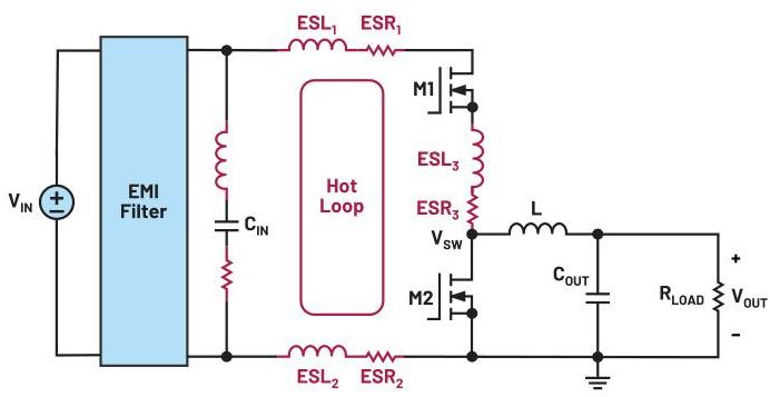
Figure 1. A buck converter with hot loop ESRs and ESLs.
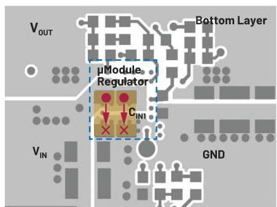
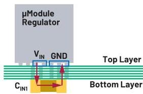
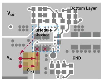
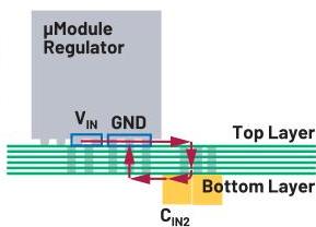
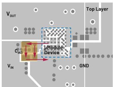
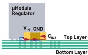
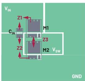
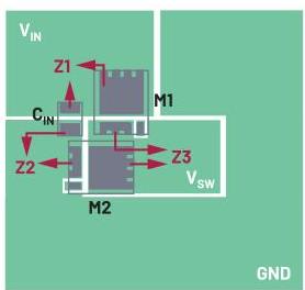
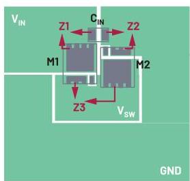
In this section, the impacts of $C_{mathrm{IN}}$ position are investigated based on ADI’s LTM4638 uModule regulator demo board DC2665A-B. The LTM4638 is an integrated 20 $V_{mathrm{IN}}$, 15 A step-down buck converter module in a tiny 6.25 mm x 6.25 mm x 5.02 mm BGA package. It offers high power density, fast transient response, and high efficiency. The module integrates a small HF ceramic $C_{mathrm{IN}}$ inside, though it is not sufficient yet, limited by the module package size. Figures 2 to 4 illustrate three different hot loops on the demo board with additional external $C_{mathrm{IN}}$. The first one is the vertical Hot Loop 1 (Figure 2), where $C_{mathrm{IN1}}$ is placed on the bottom layer just beneath the uModule regulator. The uModule $V_{mathrm{IN}}$ and GND BGA pins are connected to $C_{mathrm{IN1}}$ directly through the vias. These connections provide the shortest hot loop path on the demo board. The second hot loop is the vertical Hot Loop 2 (Figure 3), where $C_{mathrm{IN2}}$ is still placed on the bottom layer, but moved to the side area of the uModule regulator. As a result, an extra PCB trace is added to the hot loop and larger ESL and ESR are expected compared to vertical Hot Loop 1. The third hot loop option is the horizontal hot loop (Figure 4), where $C_{mathrm{IN3}}$ is placed on the top layer close to the uModule regulator. The uModule $V_{mathrm{IN}}$ and GND pins are connected to $C_{mathrm{IN3}}$ through the top layer copper without going through vias. Nevertheless, the $V_{mathrm{IN}}$ copper width on the top layer is limited by the other pinout, resulting in an increased loop impedance compared to that of vertical Hot Loop 1. Table 1 compares the extracted PCB ESRs and ESLs of the hot loops by FastHenry. As expected, the vertical Hot Loop 1 has the lowest PCB ESR and ESL.
(a)
(b)
Figure 2. Vertical hot loop 1: (a) top view and (b) side view.
(a)
(b)
Figure 3. Vertical hot loop 2: (a) top view and (b) side view.
(a)
(b)
Figure 4. Horizontal hot loop: (a) top view and (b) side view.
Table 1. Extracted PCB ESRs and ESLs in Different Hot Loops by Using FastHenry
| Hot Loop | ESR (ESR1 + ESR2) at 600 kHz (mOhm) | ESL (ESL1 + ESL2) at 200 MHz (nH) |
|---|---|---|
| Vertical Hot Loop 1 | 0.7 | 0.54 |
| Vertical Hot Loop 2 | 2.5 | 1.17 |
| Horizontal Hot Loop | 3.3 | 0.84 |
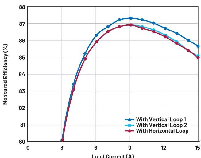
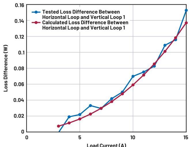
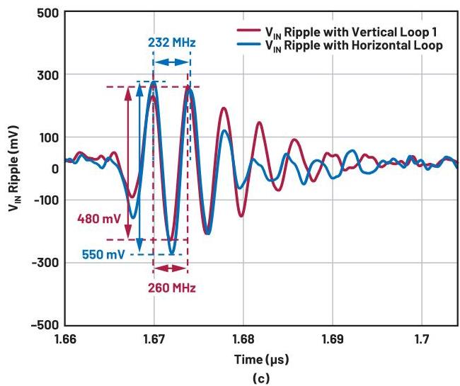
To experimentally verify the ESRs and ESLs in different hot loops, the demo board efficiency and $V_{mathrm{IN}}$ AC ripple at 12 V to 1 V CCM operation are tested. Theoretically, a lower ESR leads to higher efficiency, and smaller ESL results in higher $V_{mathrm{SW}}$ ringing frequency and lower $V_{mathrm{IN}}$ ripple magnitude. Figure 5a shows the measured efficiency. The vertical Hot Loop 1 gives the highest efficiency that corresponds to the lowest ESR. The loss difference between the horizontal hot loop and vertical Hot Loop 1 is also calculated based on the extracted ESRs, which is consistent with the testing result as shown in Figure 5b. The $V_{mathrm{IN}}$ HF ripple waveforms in Figure 5c are tested crossing $C_{mathrm{IN}}$. The horizontal hot loop has a higher $V_{mathrm{IN}}$ ripple magnitude and a lower ringing frequency, thus validating the higher loop ESL compared to the vertical Hot Loop 1. Also, because of the higher loop ESR, the $V_{mathrm{IN}}$ ripple in the horizontal hot loop damps faster than in the vertical Hot Loop 1. Furthermore, a lower $V_{mathrm{IN}}$ ripple reduces EMI and allows a smaller EMI filter size.
(a)
(b)
(c)
Figure 5. Demo board testing results: (a) efficiency, (b) loss difference between horizontal loop and vertical Loop 1, and (c) $V_{IN}$ ripple during M1 turn-on at 15 A output.
Table 2. Extracted Hot Loop PCB ESR and ESL with Various Device Shapes and Positions in FastHenry
| ESR1 (mOhm) at 2 MHz | ESR2 (mOhm) at 2 MHz | ESR3 (mOhm) at 2 MHz | ESR TOTAL (mOhm) at 2 MHz | ESR Change Rate vs. (a) | ESL1 (nH) at 200 MHz | ESL2 (nH) at 200 MHz | ESL3 (nH) at 200 MHz | ESL TOTAL (nH) at 200 MHz | ESL Change Rate vs. (a) | |
|---|---|---|---|---|---|---|---|---|---|---|
| (a) | 0.59 | 2.65 | 0.45 | 3.69 | N/A | 0.42 | 2.80 | 0.23 | 3.45 | N/A |
| (b) | 0.59 | 0.3 | 0.38 | 1.27 | -66% | 0.42 | 0.09 | 0.17 | 0.67 | -81% |
| (c) | 0.24 | 0.27 | 0.83 | 1.35 | -63% | 0.07 | 0.07 | 0.52 | 0.66 | -81% |
| (d) | 0.44 | 0.3 | 0.28 | 1.01 | -73% | 0.25 | 0.09 | 0.08 | 0.42 | -88% |
| (e) | 0.44 | 0.27 | 0.26 | 0.97 | -74% | 0.21 | 0.08 | 0.07 | 0.36 | -90% |
| (f) | 0.31 | 0.27 | 0.13 | 0.7 | -81% | 0.12 | 0.07 | 0.02 | 0.21 | -94% |
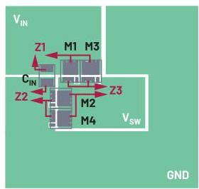
For a discrete design, the placement and package size of power FETs also have a significant impact on hot loop ESRs and ESLs. A typical half-bridge hot loop with power FETs M1 and M2 and a decoupling capacitor $C_{IN}$ is modeled and investigated in this section. As illustrated in Figure 6, popular power FET package sizes and placement positions are compared. Table 2 shows the extracted ESRs and ESLs in each case.
Cases (a) to (c) present three popular power FET placements with 5 mm x 6 mm MOSFETs. The physical length of the hot loop determines the parasitic impedance. Hence, both 90 degree shape placement in Case (b) and 180 degree shape device placement in Case (c) result in 60% ESR reduction and 80% ESL reduction because of the shorter loop paths compared to those in Case (a). Since a 90 degree shape placement shows the benefit, several more cases are investigated based on Case (b) to further reduce the loop ESR and ESL. In Case (d), a 5 mm x 6 mm MOSFET is replaced with two 3.3 mm x 3.3 mm MOSFETs in parallel. The loop length is further shortened thanks to the smaller MOSFETs footprint, leading to 7% reduction of the loop impedance. In Case (e), when a ground layer is placed under the hot loop layer, the hot loop ESR and ESL are further decreased by 2% compared to Case (d). The reason is that eddy current is generated on the ground layer, which induces the opposite magnetic field and equivalently reduces the loop impedance. In Case (f), another hot loop layer is constructed as the bottom layer. If two paralleled MOSFETs are symmetrically placed on the top layer and bottom layer and connected through vias, the hot loop PCB ESR and ESL reduction are more obvious because of the paralleled impedance. Therefore, smaller sized devices with symmetrical 90 degree shape or 180 degree shape placement on top and bottom layers lead to the lowest PCB ESR and ESL.
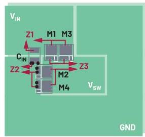
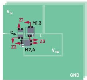
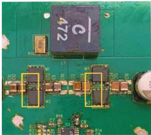
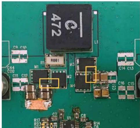
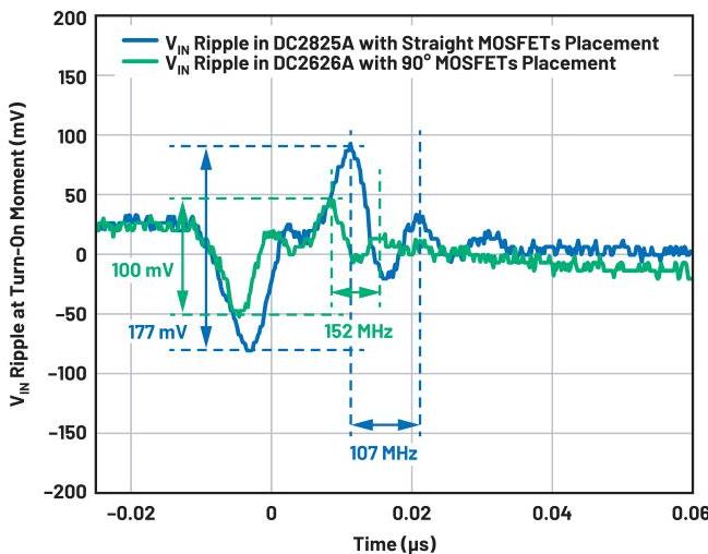
To experimentally verify the impact of the MOSFETs placement, ADI’s high efficiency, 4-switch synchronous buck-boost controller demo boards LT8390/DC2825A and LT8392/DC2626A are used. As shown in Figure 7a and Figure 7b, the DC2825A has a straight MOSFETs placement and the DC2626A has a 90 degree shape MOSFETs placement. To make a fair comparison, the two demo boards are configured with the same MOSFETs and decoupling capacitors, and tested at 36 V to 12 V/10 A, 300 kHz step-down operation. Figure 7c shows the tested $V_{IN}$ AC ripple during M1 turn-on moment. With the 90 degree shape MOSFETs placement, the $V_{IN}$ ripple has lower magnitude and higher resonant frequency, hence validating the smaller PCB ESL due to a shorter hot loop path. On the contrary, because of the longer hot loop and higher ESL, the straight MOSFETs placement results in much higher $V_{IN}$ ripple magnitude and slower resonant frequency. A higher input voltage ripple also causes a more severe EMI emission according to the EMI test results in the study of Cho and Szolusha.
(a)
(b)
(c)
(d)
(e)
(f)
Figure 6. Hot loop PCB models: (a) 5 mm x 6 mm MOSFETs in straight placement; (b) 5 mm x 6 mm MOSFETs in 90 degree shape placement; (c) 5 mm x 6 mm MOSFETs in 180 degree shape placement; (d) two-parallel 3.3 mm x 3.3 mm MOSFETs in 90 degree shape placement; (e) two-parallel 3.3 mm x 3.3 mm MOSFETs in 90 degree shape placement with ground layer; (f) symmetrical 3.3 mm x 3.3 mm MOSFETs on top and bottom layers in 90 degree shape placement.
(a)
(b)
(c)
Figure 7. (a) LT8390/DC2825A hot loop with straight MOSFETs placement; (b) LT8392/DC2626A hot loop with 90 degree MOSFETs placement; (c) $V_{IN}$ ripple waveforms at M1 turn-on.
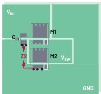
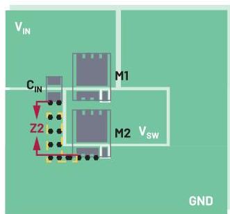
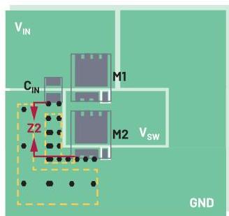
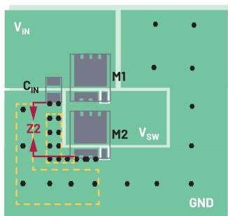
The vias placement in the hot loop also has a critical impact on the loop ESR and ESL. As shown in Figure 8, the hot loop with a two-layer PCB structure and straight power FETs placement is modeled. The FETs are placed on the top layer and the second layer is a ground plane. The parasitic impedance Z2 between $C_{IN}$ GND pad and M2 source pad is part of the hot loop and is studied as an example. Z2 is extracted from FastHenry. Table 3 summarizes and compares the simulated ESR2 and ESL2 with different via placements.
In general, adding more vias reduces the PCB parasitic impedance. However, the reduction of ESR2 and ESL2 is not linearly proportional to the number of vias. The vias close to the terminal pads give the most obvious reduction in PCB ESR and ESL. Therefore, for hot loop layout design, several critical vias must be placed close to the pads of $C_{IN}$ and MOSFETs to minimize the HF loop impedance.
(a)
(b)
(c)
(d)
Figure 8. Hot loop PCB models with (a) five GND vias placed close to $C_{IN}$ and M2; (b) 14 GND vias placed between $C_{IN}$ and M2; (c) 6 more vias placed on GND based on (b); (d) nine more vias placed on GND area based on (c).
Table 3. Extracted Hot Loop PCB ESR2 and ESL2 with Different Via Placements
| Case | ESR2 (mOhm) at 2 MHz | ESR Change Rate vs. Initial Case | ESL2 (nH) at 200 MHz | ESL Change Rate vs. Initial Case |
|---|---|---|---|---|
| Initial Case Without Vias | 2.67 | N/A | 1.19 | N/A |
| (a) | 1.73 | -35.2% | 0.84 | -29.8% |
| (b) | 1.68 | -37.1% | 0.82 | -30.8% |
| (c) | 1.67 | -37.5% | 0.82 | -31% |
| (d) | 1.65 | -38.2% | 0.82 | -31.4% |
The reduction of a hot loop’s parasitic parameters can help improve the power efficiency, lower voltage ringing, and reduce the EMI. To minimize the PCB parasitic parameters, hot loop layout designs with different decoupling capacitor positions, MOSFET sizes and positions, and via placements were studied and compared. A shorter hot loop path, smaller sized MOSFETs, symmetrical 90 degree shape and 180 degree shape MOSFETs placements, and vias close to the key components contribute to the lowest hot loop PCB ESR and ESL.
Mattan Kamon, Michael Tsuk, and Jacob White. „FASTHENRY: A Multipole-Accelerated 3-D Inductance Extraction Program.“ IEEE Transactions on Microwave Theory and Techniques, Vol. 42, 1994.
Andreas Musing, Jonas Ekman, and Johann W. Kolar. „Efficient Calculation of Non-Orthogonal Partial Elements for the PEEC Method.“ IEEE Transactions on Magnetics, Vol. 45, 2009.
Ren Ren, Zhou Dong, and Fei Fred Wang. „Bridging Gaps in Paper Design Considering Impacts of Switching Speed and Power-Loop Layout.“ IEEE, 2020.
Yonghwan Cho and Keith Szolusha. „4-Switch Buck-Boost Controller Layout for Low Emissions—Single Hot Loop vs. Dual Hot Loop.“ Analog Dialogue, Vol. 55, July 2021.
Henry J. Zhang. „PCB Layout Consideration for Non-Isolated Switching Power Supplies.“ Analog Devices, Inc., 2012.
Christian Kueck. „Power Supply Layout and EMI.“ Analog Devices, Inc., 2012.
Jingjing Sun: Jingjing Sun received a Ph.D. degree in electrical engineering from the University of Tennessee at Knoxville in 2022. After graduating, she joined the Power Product Group at Analog Devices in the California Bay Area. Jingjing is currently a senior applications engineer supporting uModule products for multimarket applications.
Ling Jiang: Ling Jiang received a Ph.D. degree in electrical engineering from the University of Tennessee at Knoxville in 2018. After graduating, she joined the Power Products Group at Analog Devices in the California Bay Area. Ling is currently an applications manager supporting uModule products for multimarket applications.
Henry Zhang: Henry Zhang is ADI’s Power by Linear applications director. He received a B.S.E.E. degree from Zhejiang University, China in 1994 and his M.S. and Ph.D. degrees in electrical engineering from Virginia Polytechnic Institute at State University, Blacksburg, Virginia in 1998 and 2001, respectively. He has been with Linear Technology (now part of ADI) since 2001.