This is Part 2 of a series of three articles that provide LTspice EMC and signal integrity simulation models. In „How to Get the Best Results Using LTspice for EMC Simulation—Part 1“, we provided LTspice simulation tools for power supply components, conducted emissions, and immunity.
In Part 2, we will present a combination of LTspice and C-based programs to help the designer understand and improve wired network signal integrity. These tools will help the designer avoid multiple lab test iterations and expensive hardware redesigns. Simulation models are provided for compliance with fieldbus communications (RS-485, RS-232), high speed backplane (LVDS), the ubiquitous USB standard, and the new single-pair Ethernet (SPE) enabling power delivery over data line (PoDL).
Signal integrity is much more than just having a working link for your prototype. Even if your link seems to be working, it’s advisable to perform an in-depth check of your signal quality, for the following reasons:

Figure 1. An example of analysis performed with LTspice.
This article will help you to answer key questions such as:
After reading this article, you should be able to:
The eye diagram provides a convenient way to assess the conformity of a signal on either the transmitter or receiver side. The eye diagram is a time-based representation of the signal.
This representation uses persistence to analyze a large number of symbols and make sure that signal levels, jitter, and rise time are appropriate.
LTspice features some of the tools required for an eye diagram analysis, but to perform a full featured analysis there are extra steps to implement.
LTspice provides an efficient way to play a test vector in your simulation. Playing a large amount of data is mandatory to provide good coverage of a situation that can lead to nonconformities.
Some nonconformities will show up in very specific situations such as:
This means, for example, that if the data is generated using a random function you might have to use thousands of symbols to make sure you encounter a specific 11 consecutive high level.
The PWL data format that LTspice expects is shown in Figure 2.

Figure 2. The file format of a PWL test vector.
Where:
// initialize
fprintf (pFile, "%dnt0n", 0, initialVoltage);
fprintf (pFile, "%dnt0n", DELAY, initialVoltage);
// loop for every sample
for (sample = 0; sample < NUMBER_OF_SAMPLES; sample++)
{
// Compute a sample
logicLevel = rand() % 2;
// print sample
if (logicLevel == 0)
{
fprintf (pFile, "%fnt%5.2fn", (sample*symbolTime) + DELAY + transitionTime, voltageLow);
fprintf (pFile, "%fnt%5.2fn", ((sample+1)*symbolTime) + DELAY - transitionTime, voltageLow);
printf ("%fnt%5.2fn", (sample*symbolTime) + DELAY, voltageLow);
}
else
{
fprintf (pFile, "%fnt%5.2fn", (sample*symbolTime) + DELAY + transitionTime, voltageHigh);
fprintf (pFile, "%fnt%5.2fn", ((sample+1)*symbolTime) + DELAY - transitionTime, voltageHigh);
printf ("%fnt%5.2fn", (sample*symbolTime) + DELAY, voltageHigh);
}
There are many options to generate test vectors. For our simulations we picked the C programming language.
With a few lines of code, you can easily generate large test vectors ready to inject into your simulation. Figure 3 presents an extract of the code used to generate the test vector and Figure 4 presents the waveform generated by the C program.

Figure 3. An extract of the code used to generate a test vector.
Figure 4. A generated test vector using C program.
Concepts used in wired communications, such as bit stuffing, can be implemented with a few lines of code as illustrated in Figure 5.
// Max consecutive identical symbol (for droop)
#define MAX_CONSECUTIVE_0 7
#define MAX_CONSECUTIVE_1 10
[...]
if (consecutiveHigh > MAX_CONSECUTIVE_1)
{ printf("Hit Max 1 limit - Bit stuffing a Zeron"); logicLevel = 0; consecutiveHigh = 0; }
if (consecutiveLow > MAX_CONSECUTIVE_0)
{ printf("Hit Max 0 limit - Bit stuffing a Onen"); logicLevel = 1; consecutiveLow = 0; }
Figure 5. Code is provided in the links of this article.
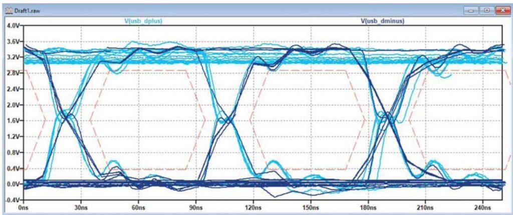
Using real-world data and importing the data into LTspice is also possible. Once the data is acquired with your regular laboratory equipment you can import it with only a few steps.
For example, Figure 6 is a capture of a USB 1.0 communication performed with an oscilloscope.

Figure 6. A USB signal captured using laboratory equipment.
Figure 7 is a typical example of a dataset saved by an oscilloscope (the exact format might differ but the given rules to import the data to LTspice will still apply).

Figure 7. Raw data of the captured USB signal.
To use this data set in an LTspice simulation, a few modifications are needed:
Then your data is ready for use within LTspice.

Figure 8. A USB signal imported in LTspice.
To use your generated PWL file you can add a voltage source and file path to your design, as shown in Figure 9.

Figure 9. A PWL option for the voltage source.
Both absolute and relative file paths will work, however, usage of relative paths is advisable as this makes your simulation portable and ready to share with your colleagues.

Figure 10. An example of a relative path.
To benefit from the full potential of this well-hidden feature of LTspice, you’ll first have to run your simulation.

Figure 11. Right click in this area to enable eye horizontal axis properties.
Once the simulation is finished and your signals are displayed, right click on the horizontal (time) axis.
A dialog will pop up, displaying an eye diagram button as shown in Figure 12.

Figure 12. The location of the eye diagram option.
This pop-up window allows you to enable and tune the eye diagram display, with self-explanatory parameters.

Figure 13. A setup of the eye diagram.
Upon validation your display will look like Figure 14.

Figure 14. An eye diagram display.
To simplify the assessment of signal integrity, the eye diagram can be associated with an eye diagram mask. An eye diagram mask is not a standard LTspice function, however, it is still possible to implement it (like the EMC limit line in Article 1).
The specification of the eye diagram is a standard, so most of the mask can be assessed from a reduced set of variables as described in Figure 15.

Figure 15. An eye diagram and an eye diagram mask.
The following list defines the letters A to E in the eye diagram mask:
In Part 1 of this article series, we described how to use drawing elements to display EMC limit lines over an FFT spectrum. In this article we show how to use the same tools to draw an eye diagram mask.
The generation of the eye diagram is more complex compared to generating and adding an EMC limit line. For eye diagrams, we use a webpage with JavaScript to generate the eye diagram definition, which can then be pasted into the plot setting file (*.plt) of your LTspice signal display. This JavaScript program, as shown in Figure 16 is available for the engineer to complete their design.
Eye diagram definitions for common wired interface standards are already provided as presets. By clicking on each radio button, the fields are filled automatically with typical values.
Figure 16. Presets of the eye diagram generator.
Fine tuning or implementation of your eye definition is also possible using the provided fields.

Figure 17. Eye mask input fields.
Corresponding plot setting commands are generated as you click on the update button. These lines are ready to be added to your plot settings file, following the method described in Part 1 of this article series.

Figure 18. Plot settings generated by the webpage.
Adjustments to the number of eyes to draw and the LTspice delay setting might be necessary to get the best display, as shown in Figure 19.

Figure 19. Plot settings generated by the webpage applied to waveforms.
The components we use in our designs include wide tolerances, and by calculation, we can check whether or not these tolerances will be problematic. But when designs include hundreds of components, pen and paper or spreadsheet manual approaches are time consuming and may not capture important parameters. Using a narrower tolerance is possible for some devices, but picking the whole bill of materials in low tolerance components will cause price and availability issues, and will not account for the effects of aging or temperature dependency.
For the purpose of validating a design over its tolerances, spice and by extension LTspice feature several amazing tools.
The following sections present techniques for tolerance analysis using Monte Carlo and Gaussian distributions as well as the worst-case analysis within LTspice.

Figure 20. Distribution of randomized values for the three main methods.
To compare the relevance and exhaustivity in a real use case we picked the following example, based on the work of Graber this setup shows a simulation circuit for the SPE 10Base-T1L standard (10SPE) physical layer or MDI. The simulation circuit shown in Figure 21 includes termination resistance of 100 +/-10% for Analog Devices‘ ADIN1110 or ADIN1100 10BASE-T1L Ethernet PHY/MAC-PHY.
Signal coupling capacitance, power coupling inductors, common mode choke, and other EMC protection components are modeled. For some components, the recommended component value and tolerance range are added.
Syntax for the return loss plot is:
(100+1/I(V1))/(100-1/I(V1))
A Monte Carlo simulation takes a random value from the tolerance range of each specified component in your simulation circuit. All values within the component tolerance range have an equal probability for circuit simulation. LTspice includes a convenient built-in Monte Carlo function with a simple syntax.
For example, to create a 100 Ohm resistor with 10% tolerance, you need to use the following syntax:
{mc(100R, TolA)}
.param TolA = 0.10
Table 1. Definition of Component Values and Tolerances with Monte Carlo Method
| Designator | Range | Syntax of Component Value (Monte Carlo) |
|---|---|---|
| R1 | 90 Ohm to 110 Ohm | {mc(100, TolA)} |
| C2, C3 | 200 nF to 600 nF | {mc(400 nF, TolB)} |
| L1 | 500 uH to 1500 uH | {mc(1000 uH, TolC)} |
| L2, L3 | 0 nH to 500 nH | {mc(250 nH, TolD)} |
| C6 | 0 pF to 200 pF | {mc(100 pF, TolE)} |
The circuit described in Figure 21 can be used to simulate return loss, which is a measure of all signal reflections likely to occur.
Return loss is caused by impedance mismatches at all locations along a cable link. Return loss is expressed in decibels and is of particular concern for high data rate or long cable reach (1700 m) communications used in 10BASE-T1L.

Figure 21. Common test circuit for Gaussian, worst case, and Monte Carlo-based on reference.
To add the MDI return loss limit line to your plot (red line shown in Figure 23), from the Plot Settings Menu hit Save Plot Settings.
Open the .PLT file using a standard text editor. Copy and paste the line definition syntax as shown in the Excel file (Figure 22).
Table: LTSpice MDI Return Loss Mask
| Start Freq | End Freq | RL Start | RL Stop | Line def for LTSPICE plot settings file |
|---|---|---|---|---|
| 100000 | 200000 | -14.562 | -20 | Line:“dB“ 4 0 (100000,0.18660574063097) (200000,0.1) |
| 200000 | 1000000 | -20 | -20 | Line:“dB“ 4 0 (200000,0.1) (1000000,0.1) |
| 1000000 | 10000000 | -20 | -3.3 | Line:“dB“ 4 0 (1000000,0.1) (10000000,0.683911647281429) |
Figure 22. Line definition for LTspice plot settings file.
To obtain identical figures in your simulations please ensure that you right click the waveform, and then click the Don’t Plot Phase button.
The Monte Carlo simulation is a relevant way to assess the compliance of an electronic design over its tolerance range, it is very likely to suit the needs of most designers while keeping the number of simulations runs reasonable.

Figure 23. Differential return losses of a SPE termination—128 runs of Monte Carlo distributed parameters.
The worst-case simulation function is not a built-in function of LTspice. However, you can implement functions to simulate worst case, as detailed in the work of Joseph Spencer and Gabino Alonso.
Both .func binary(run,index) and .func wc(nom,tol,index) functions are needed to perform simulations according to the worst-case scenario, you need to place them on your LTspice schematic sheet as a SPICE directive.
.func binary(run,index) floor(run/(2**index))- 2*floor(run/(2**(index+1)))
.func wc(nom,tol,index) if(run==numruns,nom, if(binary(run,index),nom*(1+tol),nom*(1-tol)))
In order to use these functions, you need to:
.param numruns = 129
{wc(100R, 0.1, 0)}
Where:
Run the simulation circuit shown in Figure 21 with the expressions from the following table instead of static component values:
Table 2. Definition of Component Values and Tolerances with Worst-Case Method
| Designator | Range | Syntax of Component Value (Worst-Case) |
|---|---|---|
| R1 | 90 Ohm to 110 Ohm | {wc(100, TolA, 0)} |
| C2 | 200 nF to 600 nF | {wc(400 nF, TolB, 1)} |
| C3 | 200 nF to 600 nF | {wc(400 nF, TolB, 2)} |
| L1 | 500 uH to 1500 uH | {wc(1000 uH, TolC, 3)} |
| L2 | 0 nH to 500 nH | {wc(250 nH, TolD, 4)} |
| L3 | 0 nH to 500 nH | {wc(250 nH, TolD, 5)} |
| C6 | 0 pF to 200 pF | {wc(100 pF, TolE, 6)} |
Results are displayed in the waveform plot Figure 24.
The MDI return loss mask limit line is added by editing the plot settings file as described previously.
Steve Knudtsen provides a concise overview of the benefits and limitations of using worst-case analysis for system design.
The worst-case analysis is a common approach where component parameters are adjusted to their maximum tolerance limit.
Limitations of a worst-case approach include results that do not match commonly observed results: to observe a system exhibiting worst-case performance would require the assembly of a very large number of systems.
If systems are designed for worst-case conditions, then components selection can be expensive.
However, using both worst case in conjunction with Monte Carlo or Gaussian simulation can yield valuable system insights.

Figure 24. Differential return losses of a SPE termination: 128 runs of worst-case distributed parameters.
Worst-case analysis is best suited for a gross validation of behavior when simulations are very long and when nominal behavior is already validated.
LTspice includes a built-in Gaussian function, where the centered values have a higher probability of occurring, this Gaussian function has a simple syntax.
{nominal_value*(1+gauss(tolerance/sigma))}
Adjustments according to the standard deviation parameter sigma of the Gaussian distribution can be performed using the following expressions in Table 3.
Table 3. Definition of Component Values and Tolerances with Gaussian Distribution Method
| Expression Used | Fraction of Samples within Tolerance |
|---|---|
| {nom*(1+gauss(tol/1))} | 68.2% (1 sigma) |
| {nom*(1+gauss(tol/2))} | 95.4% (2 sigma) |
| {nom*(1+gauss(tol/3))} | 99.7% (3 sigma) |
| {nom*(1+gauss(tol/4))} | 99.99% (4 sigma) |
Or using a more graphical representation:

Figure 25. Gaussian distribution of samples vs. sigma.
For example, to create a 100 Ohm resistor with 10% tolerance, and 4 sigma probability of value within tolerance you need to use the following syntax:
{100R*(1+gauss(TolA/4))}
.param TolA = 0.10
Figure 26 provides the result of 128 runs of the simulation provided in Figure 19, with Gaussian distributed parameters using 4 sigma.

Figure 26. Differential return losses of a SPE termination: 128 runs of Gaussian distributed parameters.
The Gaussian distribution is very often the most relevant way to simulate the variations of an electronic design.
The Gaussian distribution of parameters around a nominal value remains the most natural way to study the impact of tolerances.
Unfortunately, this comes at a price. To be exhaustive, you will need a large number of simulation runs.
This distribution will also pick values outside of the tolerance range, omitting the sorting and binning operations performed by component manufacturers.
Replacement of several field buses is possible using the 10BASE-T1L Ethernet standard. The same cable can be used for both traditional fieldbus and 10BASET1L, which is a simple balanced copper pair used for full duplex communication and for powering the end-powered device (PD). While the same cable can be reused, the physical layer communication transceiver (PHY) and passive components must change to meet the 10BASE-T1L standard.
Most validation of 10BASE-T1L signal integrity within LTspice can be performed with a similarly shaped signal.
Table 4. Range of Single-Pair Ethernet Depending on Transmit Signal Amplitude
| Transmit Signal Amplitude | Estimated Range |
|---|---|
| 2.4 VPP | 1000 m to 1700 m |
| 1.0 VPP | 200 m |
The encoding used is PAM3, for pulse amplitude modulation 3 levels. Depending on the desired reach and capabilities of the endpoints, the transmit signal amplitude can be adjusted to either 1 V or 2.4 V.
On the cable side, the signal rise is 53.33 ns for a -1 to +1 transition, and the fall time is the same.
Slew rate is deemed constant so 0 to 1, 1 to 0, -1 to 0 and 0 to -1 should have a nominal transition time of 26.66 ns.
To generate such a test vector, we will use the code in Figure 27.
That will output a test vector of 5000 PAM3 symbols in a PWL format.
By feeding this test vector to our schematic, we are able to validate the various parameters such as minimal coupling, interwinding capacitance, and many more.
Figures 28, 29, and 30 show the transformer-based termination for a 10BASE-T1L link, the output of a PWL source voltage file, and an eye diagram display of the PWL voltage source and cable side differential voltage. This can be used for conformance testing to the 10BASE-T1L standard.
// loop for every sample
for (sample = DELAY; sample < (NUMBER_OF_SAMPLES+DELAY); sample++)
{
// Compute a sample
previousLogicLevel = logicLevel;
logicLevel = (rand() % 3);
transition = abs((previousLogicLevel - logicLevel));
switch (transition)
{
case 2 : // +1 to -1 transition or +1 to -1 transition
fprintf (pfile, "%Et%5.2fn", (sample*M_G_PERIOD), busvoltage[previousLogicLevel]);
fprintf (pfile, "%Et%5.2fn", (sample*M_G_PERIOD)+(M_G_RISE), busvoltage[logicLevel]);
break;
case 1 : // transition to nearby state (-1 <-> 0 <-> 1)
fprintf (pfile, "%Et%5.2fn", (sample*M_G_PERIOD)+((1.0*M_G_RISE)/4.0), busvoltage[previousLogicLevel]);
fprintf (pfile, "%Et%5.2fn", (sample*M_G_PERIOD)+((3.0*M_G_RISE)/4.0), busvoltage[logicLevel]);
break;
case 0 : // no change in value
fprintf (pfile, "%Et%5.2fn", (sample*M_G_PERIOD), busvoltage[logicLevel]);
break;
default :
break;
}

Figure 27. An extract of the code used to generate PAM3 test vector.
Figure 28. Transformer-based termination with PAM3 PWL test vector.

Figure 29. An output of the PWL voltage source.

Figure 30. Eye diagram display of the PWL voltage source and cable side differential voltage.
LTspice is a powerful and free simulation tool, which can be used in conjunction with waveform generators using standard C and JavaScript code. The end result is a powerful wired communication signal integrity tool that can be used to save time with lab experiments, guide end product design, and reduce time to market for product developments. ADI and Wuerth Elektronik will provide this tool for engineers to design their wired links and help with understanding new standards such as 10BASE-T1L SPE.