This article presents the steps needed to carry out a theoretical analysis on the noise performance for a high speed wide bandwidth signal chain. Although a specific signal chain is chosen for the analysis, the steps highlighted can be considered valid for any type of signal chain. Five main phases are suggested: declaring the assumptions, drawing a simplified schematic of the chain signal, calculating the equivalent noise bandwidth for each of the signal chain blocks, calculating the noise contribution at the output of the signal chain for all blocks, and adding all noise contributions. The analysis shows how simple math can be used to describe all noise contributions. Gaining an understanding of how each block contributes to the overall noise allows the designer to appropriately modify the design (for example, choice of components) to optimize its noise performance.
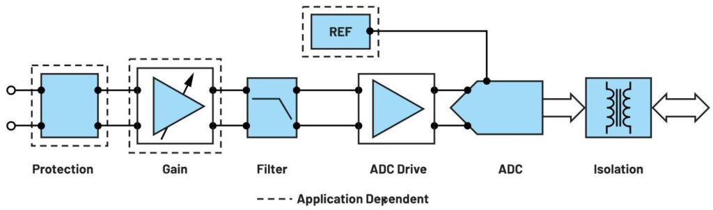
When designing a measurement signal chain, it is important to work through a noise analysis to determine if the signal chain solution will have low enough noise so that the smallest signal of interest can easily be extracted. A thorough noise analysis can save time and money during the production process. This article will outline the main steps necessary to carry out a signal chain noise analysis. We will use an example of the power optimized current and voltage measurement signal chain on the Analog Devices precision wide bandwidth technology page.
Signal chain options for measuring wide bandwidths up to 1 MHz for noise performance to support AC and/or DC analysis
| Noise and Bandwidth Optimized | Power Optimized | Density Optimized | |||
|---|---|---|---|---|---|
| Protection | Gain | ADC Driver | ADC | Voltage Reference | Isolation |
| ADG5421F +/-60 V fault protection and detection, 11 Ohm RON, dual SPST switch | LTC6373 36 V full differential programmable gain instrumentation amplifier with 25 pA input bias current | ADA4945-1 High speed, +/-0.1 uV/degC offset drift, fully differential ADC driver | LTC2387-18 LTC2387-16 15 MSPS, 18/16 bits | LTC6655 0.25 ppm noise, low drift precision references | ADN4654 5 kV rms and 3.75 kV rms, dual-channel LVDS gigabit isolators |

Figure 1. A precision wide bandwidth current/voltage measurement power optimized signal chain.
The analysis is broken into five main steps:
For the noise analysis, or any analysis performed on a signal chain circuit, it is important to outline the assumptions made for each block in the signal chain. Outlined are some of the assumptions made for this work:

Figure 2. A simplified signal chain.
From the signal chain solution (see Figure 1) a simplified schematic is generated (see Figure 2) for each of the following stages:
We can also note:
where
In this section we will calculate the equivalent noise bandwidth and noise contribution of all blocks individually.
The equivalent noise bandwidth (ENB) is the bandwidth of a brick wall filter that produces the same integrated noise power as the implemented filter.^3
The ENB for the signal chain blocks is calculated by:
For a single-pole system:
For the ADC input RC filter (2-pole system):
Note: this formula is only suitable for the combination of a 2-pole filter generated by this ADC input RC filter and ADC sampling RC network. When using different filter combinations there may be different considerations required.
(1.57 = pi/2)
Table 1. Noise Bandwidth Ratio vs. Poles
| Number of Poles | Noise Bandwidth Ratio |
|---|---|
| 1 | 1.57 |
| 2 | 1.22 |
| 3 | 1.16 |
| 4 | 1.13 |
| 5 | 1.11 |
The following analysis applies when a passive filter is used for the signal filter, as shown in Figure 3.
Note: For this analysis in the signal filter R_filter = R_G = R_driver / 2.
This is done to avoid gain at the driver stage, as we only want gain to occur in the gain block. Also R_driver = R_F as shown in Figure 4.
Noise produced by the gain block is filtered by the filter block, which has much lower bandwidth than the filter generated by the ADC drive output RC network and the ADC input sampling network.
ENB = bandwidth x pi / 2
noise_gain_stage = NSD x PGA_gain x sqrt(ENB)
The NSD value considers all the noise sources of the gain block and is given in the data sheet.

Figure 3. Schematic sections for noise analysis.

Figure 4. Setting resistor values for noise analysis.
Noise generated by the filter resistors (R_filter) is filtered by the filter itself, which has much lower bandwidth than the combined filter generated by the ADC input RC filter and the ADC sampling RC.
noise_signal_filter = sqrt(2 x 4 x k x T x (R_driver / 2) x ENB) [V rms]
The 2 is related to the differential scheme.
Noise generated by the amplifier resistors (R_driver and R_driver/2 highlighted in Figure 4) is filtered by the combined filter that exists in the next two blocks of the signal chain.
This is a second-order filter consisting of the ADC input RC filter and the ADC sampling RC.
ENB = 1.22 / (2 x pi x R_ADC_filter x (C_ADC_filter + C_ADC_sampling))
noise_driver_amp_input_resistors = sqrt(2 x 4 x 4 x k x T x R_driver/2 x ENB) [V rms]
The 2 is related to the differential scheme.
The 4 is related to the noise gain: (R_driver / (R_driver/2))^2 = 2^2
noise_driver_amp_feedback_resistors = sqrt(2 x 4 x k x T x R_driver x ENB) [V rms]
These are combined in the same step as follows:
Noise generated by the amplifier driver is filtered by the combined filter generated by the ADC input RC filter and the ADC sampling RC.
Second-order filter
noise_driver_amp = NSD_driver x sqrt(9 x ENB) [V rms]
The 9 is related to the amplifier noise gain: (1 + R_driver / (R_driver/2))^2 = 3^2
Noise generated by the resistor in the ADC input RC filter network is filtered by the combined filter generated by the ADC input RC filter and the ADC sampling RC.
Second-order filter

Figure 5. Summary sheet.
Table 2. Individual Noise Sources of a Differential Signal Chain
| Block | Noise Formula |
|---|---|
| Gain Block | noise_gain_stage = NSD x PGA_gain x sqrt(ENB) |
| Signal Filter | noise_signal_filter = sqrt(2 x 4 x k x T x R_driver/2 x ENB) [V rms] |
| ADC Driver | noise_driver_amp_resistors = sqrt(2 x (R_F/R_G)^2 x 4 x k x T x R_G x ENB + 2 x 4 x k x T x R_F x ENB); noise_driver_amp = NSD_driver x sqrt((1 + R_F/R_G)^2 x ENB) |
| ADC Input RC Filter | noise_ADC_input_RC_filter = sqrt(2 x 4 x k x T x R_ADC_input_filter x ENB) [V rms] |
| ADC | noise_ADC = (full scale) / (2 x sqrt(2) x 10^(SNR/20)) |

Figure 6. Worked example.
Table 3. Noise Contribution of the Different Stages from the Example in Figure 6
| Gain | Noise gain stage LTC6373 | Noise signal filter | Noise driver amp resistors | Noise driver amp ADA4945 | Noise ADC input RC Filter | Noise ADC LTC2387 | Noise total (RSS Method) |
|---|---|---|---|---|---|---|---|
| 0.25 | 8.30 | 2.27 | 61.9 | 47.6 | 7.99 | 45.9 | 91.3 |
| 0.5 | 10.5 | 2.27 | 61.9 | 47.6 | 7.99 | 45.9 | 91.6 |
| 1 | 14.8 | 2.27 | 61.9 | 47.6 | 7.99 | 45.9 | 92.2 |
| 2 | 19.3 | 2.27 | 61.9 | 47.6 | 7.99 | 45.9 | 93.0 |
| 4 | 30.1 | 2.27 | 61.9 | 47.6 | 7.99 | 45.9 | 95.8 |
| 8 | 53.3 | 2.27 | 61.9 | 47.6 | 7.99 | 45.9 | 105 |
| 16 | 101 | 2.27 | 61.9 | 47.6 | 7.99 | 45.9 | 136 |
*Above measurements are all uV rms
R_filter = R_G = R_driver/2 = 250 Ohm, R_driver = R_F = 500 Ohm, R_ADC_filter = 25 Ohm
By following these steps, the designer will be able to analyze and calculate the noise performance of the chosen signal chain. The analysis provides useful insights on how different components in the signal chain affect the noise performance and how these could be minimized (for example, changing resistors‘ size, changing a component, or minimizing equivalent noise bandwidths). Therefore, the designer can create a proposal that ensures the signal chain extracts the smallest signal of interest, which helps save time and money.
There is an option of using an active filter instead of a passive filter, as shown in Figure 7.
Choosing whether to use an active or passive filter in the signal chain will depend on the applications. The active filter used in the analysis had low current consumption and low noise. However, it may be unsuitable for some applications as its distortion performance is not as good over frequency.
If the active filter is chosen, it is necessary to make changes to the calculations:
Active filter:
noise_active_filter = sqrt(2 x 4 x k x T x R_filter x ENB) [V rms]
The 2 is related to the differential scheme.
When the active filter version is used there is noise from the filter amp, which forms part of the active filter. This is not necessary for use with the passive filter circuit as no filter amp is used.
Active filter:
noise_driver_amp_input_resistor = sqrt(2 x 1 x 4 x k x T x R_driver x ENB) [V rms]
The 2 is related to the differential scheme.
Note: the noise gain at the amp driver in the active filter circuit is 1: (R_driver / R_driver)^2 = 1^2
noise_driver_amp_feedback_resistor = sqrt(2 x 4 x k x T x R_driver x ENB) [V rms]
The 2 is related to the differential scheme.
These are combined as follows:
Active filter:
noise_driver_amp = NSD_driver x sqrt(4 x ENB) [V rms]
The 4 is related to the amplifier noise gain: (1 + R_driver / R_driver)^2 = 2^2
This is specific to the amplifier driver being used.
All other calculations remain as described.

Figure 7. Active filter configuration.
Pasquale Delizia: Pasquale Delizia received a master’s degree in electronic engineering from the Polytechnic University of Bari, Italy, in 2006 and a Ph.D. degree in microelectronics from the University of Lecce, Italy, in 2010. He was awarded an M.B.A. from the Henley Business School, University of Reading, in 2021. Since 2010, he has been part of the Precision Converter Technology Group at Analog Devices. After working on precision converter architectures, he transitioned into a marketing role within the same group. He can be reached at .
Rose Delaney: Rose Delaney is an electrical and electronics engineering undergraduate student at University College Cork, Ireland. She joined Analog Devices as a product applications co-op student in 2021 in the Precision Technology Group.