This application note aims to explain the fundamentals and motivation of using a system with Power over Data Line capabilities. Some of the advantages of using a system with these capabilities will be shown. While additional circuits will be required to enable a system to use this, different circuits with different properties including complexity and cost will be shown to help in deciding which solution will be required. Due to the inherent complexity of this feature, simulations are recommended and the results of simulations will be compared to their corresponding measurements.
Table 1. General Terms
| Term | Description |
|---|---|
| 10BASE-T1L | 10 Mbit/s Ethernet over long-reach single pair of conductors, IEEE Std 802.3 Clause 146 |
| 10BASE-T1S | 10 Mbit/s Ethernet over short-reach single pair of conductors, IEEE Std 802.3 Clause 147 |
| BIN | Bus Interface Network |
| CMC | Common Mode Choke |
| DMC | Differential Mode Choke |
| PD | Powered Device |
| PoDL | Power over Data Line |
| PoE | Power over Ethernet, IEEE Std 802.3 Clauses 33 and 145 |
| PSE | Power Sourcing Equipment |
AN1829 – Understanding System Inherent Noise: Enabling Longer Reach and More Nodes on 10BASE-T1S Systems
AN1829 – Understanding System Inherent Noise: Enabling Longer Reach and More Nodes on 10BASE-T1S Systems
Reducing the costs of components and assembly is an important goal in most hardware designs, regardless of the end market. Power over Ethernet (PoE) enables system designers to achieve this goal by using a single cable to both transfer data and power the device. PoE reduces assembly and material costs, since only one cable must be laid out and connected. It also reduces weight, which is especially important in automotive and other transportation applications.
PoE was initially developed for Ethernet systems using CAT5 or CAT6 Ethernet cables, which contain 4 pairs of wires, and PoE implementations use multiple pairs in these cables. The goal of reducing cost and weight has driven the development of Ethernet standards that require only a single pair of conductors, such as 100BASE-T1, 10BASE-T1L and 10BASE-T1S. Older PoE standards were not designed for only a single pair of wires; Power over Data Line (PoDL) is the solution when using a single pair.
Systems using PoDL are split into two main components: the Power Supply Equipment (PSE) and the Powered Devices (PD). As the name suggests, the PSE is responsible for providing power to the devices connected on the transmission line.
The PD is the device being powered by the PSE. PSEs can be described in terms of their voltage, current and quality of provided power. In all cases, PSEs must be able to endure the in-rush current that loads the transmission line and the PD. PDs must have a circuit to separate the power supply from the data.
PoDL standards often include a negotiation protocol to ensure necessary voltage and current are provided. On engineered systems, where the devices on the bus are already known during the design phase, it is possible for the PSE to omit the communication phase. On such systems, the PSE may power the device to the predetermined power class. This is especially useful in systems used in the automotive industry because it saves time during startup.
The IEEE 802.3 working group has defined the standards for PoDL for several point-to-point single pair Ethernet variants, such as in the IEEE 802.3bu and IEEE 802.3cg standards. The IEEE 802.3cg standard defines PoDL for both 10BASE-T1L and 10-BASE-T1S point-to-point segments. One of the key advantages of 10BASE-T1S is the ability to have more than two data nodes on one mixing segment. This makes the mixing segment a switch and enables many low bandwidth devices to communicate via standard Ethernet. At the time of creation of this document, there are no PoDL standards for 10BASE-T1S multidrop mixing segments. For these networks, inspiration from other applications can be found and used instead. This can include applications based on PoE, 10BASE-T1L systems, systems using point-to-point links, RS-485 based systems, or even USB specifications. Because there are no tight constraints to uphold, every solution to PoDL for multidrop systems is potentially different and unique.
This application note will show examples of PoDL circuits that have been tested with the LAN8670 and the LAN8671, either of which can be used as a starting point for customer design.
While the IEEE PoDL and PoE specifications define the behavior characteristics required for a point-to-point link segment, multidrop networks are not covered in these specifications. For these networks, inspiration from other applications can be found and used instead. This can include applications based on PoE, 10BASE-T1L systems, systems using point-to-point segments, RS-485 based systems, or even USB specifications. Because there are no tight constraints to uphold, every solution to PoDL for multidrop systems is potentially different and unique. In this case, it is necessary to define the constraints placed on the characteristics of the PSE, the PD, and even the characteristics of the multidrop system itself. The proposed system used in the evaluation tests will be described in the following sections.
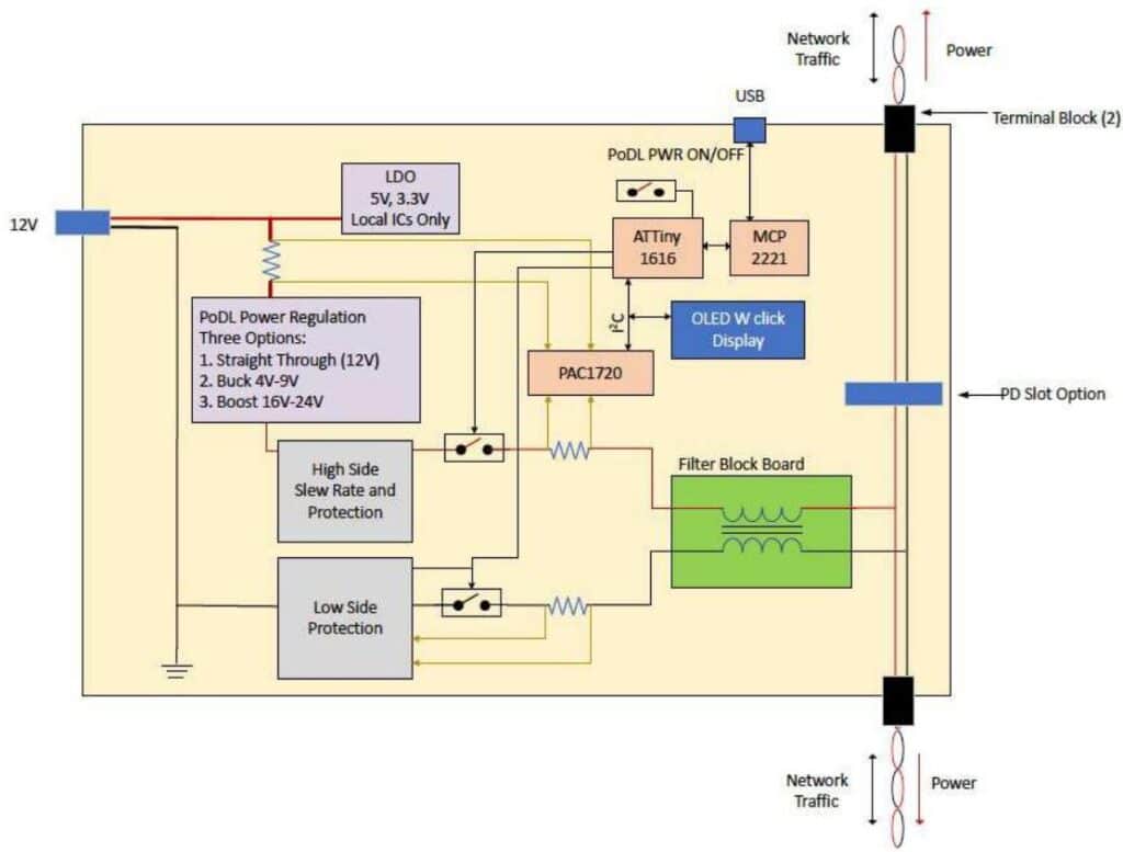
Figure 1 shows a high level block diagram of the PSE used for the evaluations. For the power source, a laboratory power supply with a stabilized 12V output was used. When different input or output voltages are required, it is possible to use a switching regulator such as a buck or boost converter. One thing to note is that if a switching regulator is used, it will potentially cause voltage ripples and produce additional noise on the output voltage. These ripples will contribute to overall system noise and should be filtered before being injected onto the network.
The green function block in Figure 1 below is implemented as an add-on board. This allows for easy testing and swapping of different power supply filter options. Three options will be evaluated: one filter uses a Differential Mode Choke (DMC), one uses two coupled inductors, and one uses two separate uncoupled inductors. The effectiveness of the filters will be analyzed by comparing these different filters to each other.

Figure 1. Outline of evaluation Power Supply Equipment.
Another important detail to note is that the PSE contains no physical layer connection for data transmissions on the network. The PSE will be used only to power the equipment on the PDs. The effects of including a PHY locally on the PSE are not taken into account here.
The cable used to transmit the data and power is a simple single twisted pair cable. This particular type of cable is often used in Microchip demonstrations and trainings. The cable used in testing is Interstate Wire WIA-2207-0/3, which is a 22 AWG wire, with a temperature rating of up to 80 degrees C and voltage rating of up to 150V. The wall thickness is 0.010 inches and with two twists per inch. Characterization tests of the cable showed that the DC resistance of the cable is 0.46 Ohm/m and the propagation delay is 6 ns/m.
The topology of the network is varied between subsequent tests and simulations. This helps test the system in different configurations. It shows whether the underlying system works in different situations or if it only works in specific situations. In the tests and simulations, four different topologies will be used. To prevent effects of node clusters affecting the network, it is recommended that nodes be placed at least 15 cm apart. Additionally, the PSE is located on the physical end of the transmission line for the topologies shown in Figure 2 below.

Figure 2. Topologies used for testing and simulation.
The first topology consists of two nodes. The first node is placed at a distance of 5m from the PSE. The second node is placed 5m from the first node. The second topology also consists of two nodes. The first node is placed at a distance of 15 cm from the PSE. The second node is placed at a distance of 15 cm from the first node.
The third topology consists of five nodes. The first is placed 5m from the PSE. The second is placed 5m from the first. The third is placed 12.5m from the second. The fourth is placed 12.5m from the third. The fifth and last is placed 14m from the fourth.
The fourth topology consists of five nodes. The first node is placed 15 cm from the PSE. Each node is then placed 15 cm from the following node. The distance between the first and second, second and third, third and fourth, and fourth and fifth is 15 cm in this topology.
The filter between the power regulator and the network greatly impacts the quality and noise of signals on the transmission network. First and foremost, this filter is intended to separate the high frequency data transmission from the low frequency power transmission. Because of this, the central component of this circuitry is a low pass filter. The following tests evaluate three different ways of using inductors to form the basis of a low pass filter connecting the PSE and network to separate power from data. The advantage of using a filter based on separate inductors is that this is the cheapest of the three used filters. However, this brings a host of disadvantages. The space required on the circuit board is possibly the largest of the filters, depending on the choice and size of components. Conversely, the noise margin for data signals is the lowest of the filters.

Figure 3. Schematic of separate inductors filter solution.
Instead of using two separate inductors, it is possible to use weakly coupled inductors or inductor arrays. This is more expensive than using two separate inductors, but the likelihood of mismatched inductors is reduced, less space is required on the circuit board depending on the choice of components, and the weak coupling between the inductors helps increase noise margin.

Figure 4. Schematic of linked inductors filter solution.
Finally, it is possible to use strongly coupled inductors, such as a Differential Mode Choke (DMC). Common mode Chokes (CMCs) can often be configured to work as DMCs. This is the most expensive solution, but it also yields the best signal quality and therefore the best noise margin for data on the transmission network.

Figure 5. Schematic of DMC filter solution.
The coupling and filtering between the PD and the network greatly affects the noise performance of each device as well. Since there are multiple devices using a similar coupling and filter, bad performance of the filter may compound the performance and reduce overall noise margins. From the point of view of the PSE, each coupling on the PD is parallel to each other. This means that for an increasing number of nodes, each additional coupling adds a further inductor parallel to the others, reducing the overall inductance of the transmission line as seen from the PSE.
Regardless of the filter type used for the power supply input on both the PSE and PD devices, a key characteristic of each device is the behavior of its power supply input. Often times, devices will also require a regulator to transform the variable voltage from the transmission line into a stable 1.8V or 3.3V supply. However, a regulator may also cause ripples and reflections to couple back into the network. To measure this, a good testing point is shown in Figure 3 and Figure 5 above. The testing point is between the locations marked as 12V PoDL and GND. The top left side of the schematic above in Figure 5 will be used as an input to a power converter to reduce the voltage to the required level for the 10BASE-T1S transceiver. The filter schematic of the power converter is part dependent and will not be shown. As a reference, when powering the device using a 12V battery and using a DMC based power filter of 47 uH, a differential noise of 91 mV and common mode noise of 43 mV were measured between the locations marked as 12V PoDL and GND. The noise was measured again on the output of the switching regulator powering the 3.3V supply voltage. This was measured as 34 mV differential noise and 29 mV common mode noise.
The number of connected devices becomes important when deciding whether to use a capacitive or inductive coupling on the Bus Interface Network (BIN) of the PD to filter out the power supply and connect data to the Ethernet ports. Capacitive coupling uses a CMC and capacitors to filter out the lower frequency power transmissions. Inductive coupling uses a transformer between the PSE network and the device to filter out the power supply part of the signal.
In both cases, only higher frequency signals are allowed to reach the device data ports, while DC and inherent low frequency standing waves are used to power the device.
In the evaluation tests, the coupling and BIN used are based on capacitive coupling. The BIN provides a capacitor in series to the TRXP and TRXN pins and a CMC across both lines. The capacitance is very small in the BIN, with the dominating factor being the inductance of the CMC.
To evaluate the effects of different configurations, placement of components and component values, various schematic variants with the three coupling filters presented earlier were tested using simulations. The setup for the different testing scenarios were derived from previously available system level templates used for data evaluation. The Keysight ADS software was used to perform these simulations. The power supply coupling filters were added to each configuration and the properties and characteristics of the inductor arrays, weakly coupled inductors, and DMC were taken from the respective manufacturers.
For each of these filters a schematic was created and simulated. Not only was the type of filter tested, but the values of the inductance was also varied to see which values lead to the best performance. As a reference, the system was also simulated without using PoDL to see what effects the power transmission has on the signal quality. The results are visualized using the eye diagram of each node of the simulation and the corresponding alien noise and jitter tolerance plot.
Since there were many simulations done during the initial phase, only the most relevant results will be discussed here. An example using only two nodes on Topology 1 and an example using five nodes on Topology 3 will be shown. The example on Topology 3 will be used as a worst case scenario, the resulting eye diagram and jitter plots will be discussed. Figure 6 below shows the results from a simulation consisting of two nodes and a power supply. The coupling between the devices and the network is realized using single, uncoupled inductors with a nominal value of 47 uH on both the positive and negative wires of the transmission line. The resulting eye diagram and jitter plot show that a large noise margin is left for the system to utilize.


Figure 6. Simulation using two 47 uH single inductors on Topology 1.


Notice: The noise and jitter plot contains the same information as the eye diagram. This plot is the superposition of each quadrant in the eye diagram normalized to show a single edge. This can also be achieved by splitting both the X- and Y-Axis into two separate parts and rotating the result to show a rising edge. The alien noise and jitter tolerance plot can be used to quickly see the worst case scenario for all participating nodes in the measurements. This is the lowest line in the plot, highlighted with red. An offset of 60 mV is subtracted from each measurement to account for the +/-30 mV signal detection threshold of the device. The y-intercept can be interpreted as the amount of jitter that is created by the system itself. This is the jitter in the system if there is no alien noise present. Since the maximum allowed jitter is 15 ns, the value of the red line at a jitter value of 15 ns indicates how much noise tolerance the system has in total. This is the amount of noise that the system may be subjected to before communications fail. If this value is below zero, it means that the system will contain at least one path failing to communicate correctly, even without external noise applied.
Figure 7 below shows a simulation of five nodes and a separate power supply. Here, each node uses a coupling to the transmission line consisting of two 68 uH inductors, one for the positive and one for the negative wire. The resulting eye diagram and jitter plot are shown.
When comparing the two results, it is obvious that the five node configuration is inherently much more sensitive to external noise than the two node configuration. This is because the topology of the system itself causes noise on the network, reducing the overall noise threshold at which communication between nodes will be disrupted. However, the noise performance is still within acceptable bounds because there is a large margin before additional noise becomes an issue, meaning that every node is able to both receive power over the transmission line and still communicate successfully with each other node in the system.

Figure 7. Simulation using 68 uH single Inductors on Topology 3.
Figure 8 below shows the topology used to test an additional configuration with eight nodes. In this configuration the PSE was moved from the end of the cable to a location between the fourth and fifth nodes. The filter between the power supply on each device and the network was realized using a 47 uH coupled inductor on each device.
Figure 9 below shows the results of the simulation of the eight node topology. The overall noise tolerance of this system is the lowest so far, but for environments with lower alien noise it is still possible to implement this system successfully.

Figure 8. 8 Node Topology.

Figure 9. 8 Node Topology Simulation.

To verify the results of the simulations and to check the behavior of the systems in a real environment, the evaluations were repeated using real hardware in a laboratory environment. The same topologies and couplings were used, and the same values for the components were used. The results of the simulations will be compared to the results of these measurements.
Figure 10 below shows the results from the measurement of the same configuration that was simulated previously. The resulting eye diagram and jitter plot of the measurements are nearly identical to the simulation results.


Figure 10. Measurements using two 47 uH single inductors on Topology 1.

Figure 11 below shows the results of the measurement of the second system that was simulated. Again, the resulting eye diagram and jitter plot are not exactly equal, but still very close to the results of the simulation.

Figure 11. Measurements using two 68 uH separate inductors on Topology 3.
In both the simulation and measurement, the second system shows much worse noise and jitter performance than the first system. However, despite this, both systems are fully functional. The second example is used as a worst case analysis of the results. An important thing to note is that the amount of external or alien noise will greatly affect the system. In a high noise environment, a high alien noise tolerance is required for the system to work properly. On the other hand, if the system is employed in an environment with little external noise, it will still remain functional even with a very low noise tolerance. Therefore, to make a valid prediction about the functionality of the system the level of alien noise must also be known.
Finally, the setup for an eight node system was tested. The topology is the same that was simulated previously. The results of the eight node measurement are shown below in Figure 12. The Alien Noise and Jitter Tolerance plot shows that the system has some noise tolerance left over. If the environment the system is placed in does not have too much noise, it will function correctly.

Figure 12. Measurements using 47 uH coupled Inductors on 8 Node Topology.

Table 2 below shows some of the inductors used in testing. One of the biggest issues when using single inductor pairs is finding equally matched inductors for each device. Using matched inductors is recommended to keep the symmetry of the differential line. If different value inductors are used, the eye diagram for the particular node will not be symmetric, reducing noise margin. Furthermore, the inductors used are only rated for a relatively low current. This may be acceptable for each PD, since it requires little power individually, but this will become an issue for the PSE when it will need to power each device simultaneously. Measurements and tests also showed that the tolerance of the components can play a major role on the workability of the solution. A minimum inductance on each node is required. If the actual inductance falls below this because the components tolerance is too high, then the system might be more susceptible to external noise.
Table 2. Component Used During Testing.
| Architecture | Nominal Inductance (uH) | Saturation Current (mA) | Rated Current (mA) | DC Resistance (mOhm) | Tolerance (%) |
|---|---|---|---|---|---|
| DMC | 47 | 300 | 250 | 806 | +/-20 |
| Single Inductors | 15 | 1100 | 850 | 252 | +/-20 |
| Single Inductors | 47 | 700 | 660 | +/-20 | |
| Single Inductors | 68 | 760 | 420 | +/-20 | |
| Coupled Inductors | 47 | 1375 | 900 | 300 | +/-20 |
| Coupled Inductors | 68 | 2220 | 1220 | 230 | +/-20 |
| Coupled Inductors | 47 | 1440 | 174 | +/-20 |
While taking the measurements during the tests described above, the connected nodes were powering the local microcontrollers. While not measuring the power consumption of each individual node, the total power consumption of the system was measured instead. The results are shown below in Table 3.
Table 3. Measured Power Consumption of System Configurations.
| Number of Nodes | Network Supply Voltage | Total Current |
|---|---|---|
| 2 | 12V | 160 mA |
| 5 | 12V | 480 mA |
| 8 | 12V | 740 mA |
Additional measurements were done for the eight node system. For this system, a load variation test was conducted. During this test, one node draws additional power to simulate cyclic power consumption of an application or transmission. To test this, a dynamic load was applied on the low voltage side of the power regulator. This dynamic load was implemented by adding a 13 Ohm resistance parallel to the rest of the node. This extra load resembled a sawtooth signal, where the current drawn steadily increased to the maximum and then rapidly returned to zero. The frequency of the signal was changed and is shown in Table 4. During these tests, the system was monitored to see if this has an impact on the noise created in the system and if communication between nodes is still possible. During any of these tests, no communication was lost and the nodes were able to transfer data as normal. No major impact on noise behavior was detected. The results of these tests are shown below.
Table 4. Load Variations for Eight Node System.
| Load Variation Frequency | Network Supply Voltage | Total Maximum Current |
|---|---|---|
| 77 Hz | 12V | 955 mA |
| 778 Hz | 12V | 962 mA |
| 180 Hz | 12V | 1004 mA |
After conducting these tests, the final step is to analyze the results. The comparison between the simulations and measurements showed that the results are nearly identical. In general, the simulations predicted that the system would behave worse than what was seen during measurements. Therefore, if the simulations show that the system performs within the acceptable range, then the real system will function as well. The system simulations and measurements showed that a fully functional system using Power over Data Line is possible.
As a reference, the system performance for all topologies was compared to the performance without using PoDL. This was also done for the eight node system. The results of these tests were compared to the corresponding system running PoDL. The result of this comparison showed that the system behavior of the systems using PoDL are very similar to the systems not using PoDL. The systems using PoDL are more susceptible to alien noise, but only by a small margin. This shows that much of the inherent noise of a system stems from the topology and interfaces to the network, both of which affect the system regardless.
While all topologies and component selections that were tested stayed within the required noise margin, clear advantages and disadvantages of each power coupling filter type were discovered. For the filter based on uncoupled single inductors, the resulting system has the lowest noise margin from the filters that were tested. This value degrades even further the lower the value of the inductance, the higher the distance, and the larger the node count become. Filters based on coupled inductors offer a good balance between costs, layout size and noise margin. Coupled inductors have a larger noise margin than separate inductors, but the best performance can be achieved using a filter based on DMCs. Systems using a filter based on DMCs will have the largest noise margin and will therefore be more robust against external noise effects. However, when a large current is required the size and cost of the DMC will greatly increase.
The simulations and tests confirm that DMCs are the most suitable components tested if a large noise margin is required. The tests show that the noise behavior of the system is very close to the behavior without the use of PoDL. However, the simulations and tests showed that some care must be taken in regards to the selection of components. For the power supply filter on each device, at least 80 uH of inductance in total are recommended. For single inductors, this means at least 40 uH on each of the positive and negative wires of the network. The PSE should also support the total power requirements of the system, potentially requiring inductors that have a higher rated current than the powered devices on the network.
Since the possible combinations of power supply voltages, regulators, coupling topology, nominal inductor value and variance, system topology and component vendors is nearly infinite, it is impossible to clearly say which combinations and setups will work. It is vital that simulations are used to assure the functionality of the desired system. This application note shows that with the right model, an entire system can be simulated such that the resulting measurements of a real system are the same as the simulations.
Furthermore, the systems shown here can be viewed as a performance floor. The examples shown here are still functional, so if a new system adheres to the electrical characteristics of its components and the simulations show similar performance to the results presented here, then this new system will also be functional.
An important conclusion to draw from this example is that system simulation is invaluable. It is imperative that the total current and voltage of each component is not exceeded and that the total system noise margin is not wholly consumed by the inherent system noise. The required margin for external noise depends largely on the expected external noise and environmental factors, if the system is expected to be subject to much alien noise then the simulations and topology of the system need to show a larger noise margin for the system to still work in that environment. Early simulation helps detect flaws in the design or topology of a desired system and allows to implement changes early in the design phase.